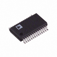
AD9226ARSZ Analog Devices Inc, AD9226ARSZ Datasheet

AD9226ARSZ
Specifications of AD9226ARSZ
Available stocks
Related parts for AD9226ARSZ
AD9226ARSZ Summary of contents
Page 1
PRODUCT DESCRIPTION The AD9226 is a monolithic, single-supply, 12-bit, 65 MSPS analog-to-digital converter with an on-chip, high-performance sample-and-hold amplifier and voltage reference. The AD9226 uses a multistage differential pipelined architecture with a pat- ented input stage and output error ...
Page 2
AD9226–SPECIFICATIONS (AVDD = 5 V, DRVDD = SPECIFICATIONS noted.) P arameter RESOLUTION ACCURACY Integral Nonlinearity (INL) Differential Nonlinearity (DNL) No Missing Codes Guaranteed Zero Error Gain Error TEMPERATURE DRIFT Zero Error 1 Gain Error 2 Gain ...
Page 3
DIGITAL SPECIFICATIONS Parameters 1 LOGIC INPUTS (Clock, DFS , Duty Cycle 1 Output Enable ) High-Level Input Voltage Low-Level Input Voltage High-Level Input Current (V = AVDD) IN Low-Level Input Current ( Input Capacitance 1 Output ...
Page 4
AD9226–SPECIFICATIONS AC SPECIFICATIONS (AVDD = 5 V, DRVDD = Parameter SIGNAL-TO-NOISE RATIO f = 2.5 MHz MHz MHz MHz 200 MHz ...
Page 5
EXPLANATION OF TEST LEVELS Test Level I. 100% production tested. II. 100% production tested at 25°C and sample tested at specified temperatures. AC testing done on sample basis. III. Sample tested only. IV. Parameter is guaranteed by design and characterization ...
Page 6
AD9226 PIN CONNECTION 48-Lead LQFP AVSS 1 PIN 1 2 AVSS IDENTIFIER AVDD 3 AVDD AD9226 NC 6 TOP VIEW CLK 7 (Not to Scale OEB ...
Page 7
DEFINITIONS OF SPECIFICATIONS INTEGRAL NONLINEARITY (INL) INL refers to the deviation of each individual code from a line drawn from “negative full scale” through “positive full scale.” The point used as “negative full scale” occurs 1/2 LSB before the first ...
Page 8
AD9226 DRVDD AVDD AVSS DRVDD DRVDD DRVSS DRVSS AVDD AVSS AVDD AVSS ...
Page 9
V, DRVDD = 3 MSPS with CLK Stabilizer Enabled, T SAMPLE V = 2.0 V, unless otherwise noted.) REF 0 –10 –20 –30 –40 –50 –60 –70 –80 –90 –100 –110 –120 0 ...
Page 10
AD9226 75 2V SPAN, DIFFERENTIAL SPAN, SINGLE-ENDED FREQUENCY – MHz –45 2V SPAN, SINGLE-ENDED –50 –55 –60 –65 –70 –75 –80 –85 – FREQUENCY – MHz 72 –40 C ...
Page 11
HARMONIC 95 85 3RD HARMONIC 75 65 2ND HARMONIC 55 100 1 10 FREQUENCY – MHz 100 2MHz 12MHz 20MHz ...
Page 12
AD9226 AD9226–Typical IF Sampling Performance Characteristics (AVDD = 5.0 V, DRVDD = 3 MSPS with CLK Stabilizer Enabled, T SAMPLE V = 2.0 V, unless otherwise noted.) REF 0 SNR = 70.2dBFS –10 SFDR = 89dBFS ...
Page 13
61.44MSPS SAMPLE –20 –30 –40 –50 –60 –70 –80 –90 –100 –110 –120 FREQUENCY – MHz 0 SNR = 65.1dBFS –10 SFDR = 59dBFS NOISE FLOOR = ...
Page 14
AD9226 THEORY OF OPERATION The AD9226 is a high-performance, single-supply 12-bit ADC. The analog input of the AD9226 is very flexible allowing for both single-ended or differential inputs of varying amplitudes that can be ac- or dc-coupled. It utilizes a ...
Page 15
AD9226 0.5V 33 VINA 15pF VINB 33 CAPT 1V VREF 0 CAPB SENSE REFCOM 1.25V AD9226 0.75V 33 VINA 49.9 15pF CAPT VINB 33 1V VREF CAPB 1.25V 10 F 0.1 F 0.75V SENSE 2.5V AD9226 ...
Page 16
AD9226 0 p-p 499 0V VINA 450 AD8138 AD9226 49.9 499 VINB 499 0 –20 –40 –60 –80 –100 –120 MHz The same midsupply potential ...
Page 17
The low-impedance VREF output can be used to provide dc bias levels to the fixed VINB pin and the signal on VINA. Fig- ure 9b shows the VREF configured for 2.0 V, thus the input range of the ADC is ...
Page 18
AD9226 AD9226 TO A DISABLE LOGIC A1 VREF CAPT 10 F 0.1 F AD9226 CAPB The actual reference voltages used by the internal circuitry of the AD9226 appear on the CAPT and CAPB pins. The voltages ...
Page 19
MODE CONTROLS Clock Stabilizer The clock stabilizer is a circuit that desensitizes the ADC from clock duty cycle variations. The AD9226 eases system clock constraints by incorporating a circuit that restores the internal duty cycle to 50%, independent of the ...
Page 20
AD9226 Digital Output Driver Considerations The AD9226 output drivers can be configured to interface with 3.3 V logic families by setting DRVDD 3.3 V respectively. The output drivers are sized to provide sufficient ...
Page 21
internal bias point on the LQFP package. It must be decoupled to ground with a 0.1 µF capacitor. The digital activity on the AD9226 chip falls into two general categories: correction logic and output drivers. The ...
Page 22
AD9226 TP5 WHT R3 10k C21 R4 C35 10 F 10k 0.1 F 10V TP2 FBEAD DUTAVDDIN TB1 2 C58 C59 22 F 0.1 F 25V AGND TB1 3 TP1 FBEAD AVDDIN TB1 1 ...
Page 23
AUXCLK T1– R11 49 MC100EL33D 8 1 AVDD VCC OUT INA 6 3 REF INB 5 4 VEE INCOM AVDD AVDD AVDD C17 R12 R13 0.1 ...
Page 24
AD9226 RP3 OTRO OTR RP3 D130 D13 RP3 D120 D12 RP3 D110 D11 RP4 C15 AVDD 10 F D100 D10 RP4 10V ...
Page 25
AD9226 ...
Page 26
AD9226 ...
Page 27
AD9226 ...
Page 28
AD9226 28-Lead Shrink Small Outline (RS-28) 0.407 (10.34) 0.397 (10.08 0.07 (1.79) 0.078 (1.98) PIN 1 0.066 (1.67) 0.068 (1.73) 0.0256 0.015 (0.38) 0.008 (0.203) SEATING 0.009 (0.229) (0.65) 0.010 (0.25) PLANE 0.002 (0.050) BSC 0.005 ...


