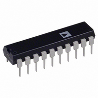
AD7703AN Analog Devices Inc, AD7703AN Datasheet - Page 14

AD7703AN
Manufacturer Part Number
AD7703AN
Description
IC ADC 20BIT LC2MOS 20-DIP
Manufacturer
Analog Devices Inc
Datasheet
1.AD7703AR-REEL.pdf
(16 pages)
Specifications of AD7703AN
Rohs Status
RoHS non-compliant
Number Of Bits
20
Sampling Rate (per Second)
4k
Data Interface
Serial
Number Of Converters
1
Power Dissipation (max)
37mW
Voltage Supply Source
Analog and Digital, Dual ±
Operating Temperature
-40°C ~ 85°C
Mounting Type
Through Hole
Package / Case
20-DIP (0.300", 7.62mm)
Available stocks
Company
Part Number
Manufacturer
Quantity
Price
Part Number:
AD7703AN
Manufacturer:
ADI/亚德诺
Quantity:
20 000
AD7703
Synchronous Self-Clocking Mode (SSC)
The SSC mode (MODE pin high) allows easy interfacing to
serial-parallel conversion circuits in systems with parallel data
communication. This mode allows interfacing to 74XX299
Universal Shift registers without any additional decoding. The
SSC mode can also be used with microprocessors such as the
68HC11 and 68HC05, which allow an external device to clock
their serial port.
Figure 15 shows the timing diagram for the SSC mode. Data is
clocked out by an internally generated serial clock. The AD7703
divides each sampling interval into 16 distinct periods. Eight
periods of 64 clock pulses are for analog settling and eight peri-
ods of 64 clock pulses are for digital computation. The status of
CS is polled at the beginning of each digital computation period. If
it is low at any of these times, then SCLK will become active
SDATA (O)
INTERNAL
SDATA (O)
DRDY (O)
DRDY (O)
CLKIN (I)
SCLK (O)
SCLK (O)
STATUS
CS (I)
CS (I)
HI-Z
HI-Z
CYCLES
HI-Z
HI-Z
CLKIN
72 CLKIN CYCLES
72
Figure 16. SSC Mode Showing Data Timing Relative to SCLK
ANALOG TIME 0
Figure 15. Timing Diagram for SSC Transmission Mode
64 CLKIN
CYCLES
DB19 (MSB)
MSB
DIGITAL TIME 0
CS POLLED
DB18
64 CLKIN
CYCLES
–14–
DB17
and the data-word currently in the output register will be trans-
mitted, MSB first. After the LSB has been transmitted, DRDY
will go high until the new data-word becomes available. If CS,
having been brought low, is taken high again at any time during
data transmission, SDATA and SCLK will go three-state after
the current bit finishes. If CS is subsequently brought low,
transmission will resume with the next bit during the subse-
quent digital computation period. If transmission has not been
initiated and completed by the time the next data-word is avail-
able, DRDY will go high for four clock cycles then low again as
the new word is loaded into the output register.
A more detailed diagram of the data transmission in the SSC
mode is shown in Figure 16. Data bits change on the falling
edge of SCLK and are valid on the rising edge of SCLK.
LSB
1024 CLKIN CYCLES
DB2
HI-Z
HI-Z
DIGITAL TIME 7
DB1
DB0 (LSB)
HI-Z
HI-Z
REV. E


