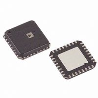
AD9237BCPZ-65 Analog Devices Inc, AD9237BCPZ-65 Datasheet - Page 21

AD9237BCPZ-65
Manufacturer Part Number
AD9237BCPZ-65
Description
IC ADC 12BIT SGL 65MSPS 32LFCSP
Manufacturer
Analog Devices Inc
Specifications of AD9237BCPZ-65
Data Interface
Parallel
Number Of Bits
12
Sampling Rate (per Second)
65M
Number Of Converters
3
Power Dissipation (max)
190mW
Voltage Supply Source
Single Supply
Operating Temperature
-40°C ~ 85°C
Mounting Type
Surface Mount
Package / Case
32-VFQFN, CSP Exposed Pad
Resolution (bits)
12bit
Input Channel Type
Differential
Supply Voltage Range - Analogue
2.7V To 3.6V
Supply Voltage Range - Digital
2.25V To 3.6V
Supply Current
64.5mA
Sampling Rate
65MSPS
Rohs Compliant
Yes
Number Of Elements
1
Resolution
12Bit
Architecture
Pipelined
Sample Rate
65MSPS
Input Polarity
Unipolar
Input Type
Voltage
Rated Input Volt
±0.5/±1/±2V
Differential Input
Yes
Power Supply Requirement
Single
Single Supply Voltage (typ)
3V
Single Supply Voltage (min)
2.7V
Single Supply Voltage (max)
3.6V
Dual Supply Voltage (typ)
Not RequiredV
Dual Supply Voltage (min)
Not RequiredV
Dual Supply Voltage (max)
Not RequiredV
Power Dissipation
270mW
Differential Linearity Error
±1.25LSB
Integral Nonlinearity Error
±2LSB
Operating Temp Range
-40C to 85C
Operating Temperature Classification
Industrial
Mounting
Surface Mount
Pin Count
32
Package Type
LFCSP EP
Lead Free Status / RoHS Status
Lead free / RoHS Compliant
Lead Free Status / RoHS Status
Lead free / RoHS Compliant, Lead free / RoHS Compliant
Available stocks
Company
Part Number
Manufacturer
Quantity
Price
Company:
Part Number:
AD9237BCPZ-65
Manufacturer:
CREE
Quantity:
101
By asserting the PDWN pin to AVDD/3, the AD9237 is placed
in standby mode. In this state, the ADC typically dissipates
20 mW. The output drivers are placed in a high impedance
state. The reference circuitry is enabled, allowing for a quick
start upon bringing the ADC into normal operating mode.
DIGITAL OUTPUTS
The AD9237 output drivers can be configured to interface with
2.5 V or 3.3 V logic families by matching DRVDD to the digital
supply of the interfaced logic. The output drivers are sized to
provide sufficient output current to drive a wide variety of logic
families. However, large drive currents tend to cause current
glitches on the supplies that can affect converter performance.
Applications requiring the ADC to drive large capacitive loads
or large fanouts may require external buffers or latches.
The length of the output data lines and loads placed on them
should be minimized to reduce transients within the AD9237;
these transients can detract from the converter’s dynamic
performance.
As detailed in Table 10, the data format can be selected for
either offset binary, twos complement, or gray code.
Operational Mode Selection
The AD9237 can output data in either offset binary, twos
complement, or gray code format. There is also a provision
for enabling or disabling the duty cycle stabilizer (DCS).
The MODE pin is a multilevel input that controls the data
format (except for gray code) and DCS state. The MODE pin
is internally pulled down to AGND by a 70 kΩ resistor. The
input threshold values and corresponding mode selections are
outlined in Table 10.
The gray code output format is obtained by connecting GC to
AVDD. When the part is in gray code mode, the MODE pin
controls the DCS function only. The GC pin is internally pulled
down to AGND by a 70 kΩ resistor.
Table 10. MODE Selection
MODE Voltage
AVDD
2/3 AVDD
1/3 AVDD
AGND (Default)
Out of Range (OTR)
An out-of-range condition exists when the analog input voltage
is beyond the input range of the ADC. The OTR pin is a digital
output that is updated along with the data output corresponding
to the particular sampled input voltage. Therefore, the OTR pin
has the same pipeline latency as the digital data. OTR is low
when the analog input voltage is within the analog input range,
and high when the analog input voltage exceeds the input range,
as shown in Figure 45. OTR remains high until the analog input
returns to within the input range and another conversion is
Data Format
Twos Complement
Twos Complement
Offset Binary
Offset Binary
Duty Cycle Stabilizer
Disabled
Enabled
Enabled
Disabled
Rev. A | Page 21 of 24
completed. By logically AND-ing OTR with the MSB and its
complement, overrange high or underrange low conditions can
be detected. Table 11 is a truth table for the overrange/ under-
range circuit in Figure 46, which uses NAND gates. Systems
requiring programmable gain condition of the AD9237 can,
after eight clock cycles, detect an out-of-range condition;
therefore, eliminating gain selection iterations. In addition,
OTR can be used for digital offset and gain calculation.
Table 11. Output Data Format
OTR
0
0
1
1
Digital Output Enable Function (OE)
The AD9237 has three-state ability. The OE pin is internally
pulled down to AGND by a 70 kΩ resistor. If the OE pin is low,
the output data drivers are enabled. If the OE pin is high, the
output data drivers are placed in a high impedance state. It is
not intended for rapid access to the data bus. Note that the
OE pin is referenced to the digital supplies (DRVDD) and
should not exceed that voltage.
Timing
The AD9237 provides latched data outputs with a pipeline delay
of eight clock cycles. Data outputs are available one propagation
delay (t
Figure 2 for a detailed timing diagram.
OTR DATA OUTPUTS
1
0
0
0
0
0
1111 1111 1111
1111 1111 1111
1111 1111 1110
0000 0000 0001
0000 0000 0000
0000 0000 0000
MSB
MSB
OTR
PD
Figure 45. OTR Relation to Input Voltage and Output Data
) after the rising edge of the clock signal. Refer to
MSB
0
1
0
1
Figure 46. Overrange/Underrange Logic
–FS – 1/2 LSB
OTR
–FS + 1/2 LSB
–FS
Analog Input Is
Within range
Within range
Underrange
Overrange
+FS – 1 LSB
OVER = 1
UNDER = 1
–FS – 1/2 LSB
AD9237
+FS


