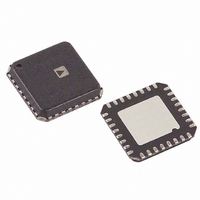
AD9237BCPZ-65 Analog Devices Inc, AD9237BCPZ-65 Datasheet - Page 3

AD9237BCPZ-65
Manufacturer Part Number
AD9237BCPZ-65
Description
IC ADC 12BIT SGL 65MSPS 32LFCSP
Manufacturer
Analog Devices Inc
Specifications of AD9237BCPZ-65
Data Interface
Parallel
Number Of Bits
12
Sampling Rate (per Second)
65M
Number Of Converters
3
Power Dissipation (max)
190mW
Voltage Supply Source
Single Supply
Operating Temperature
-40°C ~ 85°C
Mounting Type
Surface Mount
Package / Case
32-VFQFN, CSP Exposed Pad
Resolution (bits)
12bit
Input Channel Type
Differential
Supply Voltage Range - Analogue
2.7V To 3.6V
Supply Voltage Range - Digital
2.25V To 3.6V
Supply Current
64.5mA
Sampling Rate
65MSPS
Rohs Compliant
Yes
Number Of Elements
1
Resolution
12Bit
Architecture
Pipelined
Sample Rate
65MSPS
Input Polarity
Unipolar
Input Type
Voltage
Rated Input Volt
±0.5/±1/±2V
Differential Input
Yes
Power Supply Requirement
Single
Single Supply Voltage (typ)
3V
Single Supply Voltage (min)
2.7V
Single Supply Voltage (max)
3.6V
Dual Supply Voltage (typ)
Not RequiredV
Dual Supply Voltage (min)
Not RequiredV
Dual Supply Voltage (max)
Not RequiredV
Power Dissipation
270mW
Differential Linearity Error
±1.25LSB
Integral Nonlinearity Error
±2LSB
Operating Temp Range
-40C to 85C
Operating Temperature Classification
Industrial
Mounting
Surface Mount
Pin Count
32
Package Type
LFCSP EP
Lead Free Status / RoHS Status
Lead free / RoHS Compliant
Lead Free Status / RoHS Status
Lead free / RoHS Compliant, Lead free / RoHS Compliant
Available stocks
Company
Part Number
Manufacturer
Quantity
Price
Company:
Part Number:
AD9237BCPZ-65
Manufacturer:
CREE
Quantity:
101
Preliminary Technical Data
DIGITAL SPECIFICATIONS
Parameter
LOGIC INPUTS
LOGIC OUTPUTS
DRVDD = 3.3V
DRVDD = 2.5V
NOTES:
1. Output Voltage Levels measured with 5pF load on each output.
Specifications subject to change without notice.
SWITCHING SPECIFICATIONS
Parameter
CLOCK INPUT PARAMETERS
DATA OUTPUT PARAMETERS
OUT-OF_RANGE RECOVERY TIME
NOTES:
1. Valid Data Delay is measured from CLOCK 50% transition to DATA 50% transition, with 5pF load.
2. Wake-Up Time is dependant on value of decoupling capacitors, typical values shown with 0.1µF and 10µF capacitors on REFT and REFB.
Specifications subject to change without notice.
AD9237 Preliminary Technical Information – 5/18/2005
High-Level Input Voltage
Low-Level Input Voltage
High-Level Input Current
Low-Level Input Current
Input Capacitance
High-Level Output Voltage (IOH=50µA)
High-Level Output Voltage (IOH=0.5mA)
Low-Level Output Voltage (IOL=1.6mA)
Low-Level Output Voltage (IOL=50µA)
High-Level Output Voltage (IOH=50µA)
High-Level Output Voltage (IOH=0.5mA)
Low-Level Output Voltage (IOL=1.6mA)
Low-Level Output Voltage (IOL=50µA)
Max Conversion Rate
Min Conversion Rate
CLOCK PERIOD
CLOCK Pulsewidth High
CLOCK Pulsewidth Low
Output Delay
Pipeline Delay (Latency)
Output Enable Time
Aperture Delay
Aperture Uncertainty (Jitter)
Output Disable Time
Wake-Up time
Wake-Up time (Standby Mode)
1
(t
2
OD
(Sleep Mode)
1
)
ANALOG
INPUT
DATA
CLK
OUT
N-9
N-1
Temp
Full
Full
Full
Full
Full
Full
Full
Full
Full
Full
Full
Full
Full
Temp
Full
Full
Full
Full
Full
Full
Full
Full
Full
Full
Full
Full
Full
N-8
Full
N
t A
N-7
N+1
Figure 1. Timing Diagram
Test
Level
IV
IV
IV
IV
V
IV
IV
IV
IV
IV
IV
IV
IV
Test
Level
IV
V
V
V
V
V
V
V
V
V
V
V
V
V
N-6
N+2
–3–
AD9237BCPZ-20
Min
2.0
-10
-10
3.29
3.25
2.49
2.45
AD9237BCPZ-20
Min
20
50.0
15
15
N-5
N+3
Typ
2
Typ
3.5
9
6
3
1.0
0.5
2.5
tbd
1
N-4
N+4
Max
0.8
10
10
0.2
0.05
0.2
0.05
Max
1
N-3
N+5
N-2
AD9237BCPZ-40
Min
2.0
-10
-10
3.29
3.25
2.49
2.45
AD9237BCPZ-40
Min
40
25.0
8.8
8.8
N+6
N-1
Typ
2
Typ
3.5
9
6
3
1.0
0.5
2.5
tbd
1
N+7
t PD = 6.0ns MAX
N
Max
0.8
10
10
0.2
0.05
0.2
0.05
Max
1
N+8
2.0ns MIN
AD9237BCPZ-65
Min
2.0
-10
-10
3.29
3.25
2.49
2.45
AD9237BCPZ-65
Min
65
16.6
6.8
6.8
Typ
2
Typ
3.5
9
6
3
1.0
0.5
2.5
tbd
2
AD9237
Max
0.8
10
10
0.2
0.05
0.2
0.05
Max
1
REV
Units
V
V
µA
µA
PF
V
V
V
V
V
V
V
V
Units
MSPS
MSPS
ns
ns
ns
Cycles
ns
ns
ns
ps rms
ms
ns
cycles
PrF


