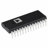
AD7862ANZ-10 Analog Devices Inc, AD7862ANZ-10 Datasheet - Page 10

AD7862ANZ-10
Manufacturer Part Number
AD7862ANZ-10
Description
IC ADC 12BIT DUAL 250KSPS 28DIP
Manufacturer
Analog Devices Inc
Datasheet
1.AD7862ARZ-10.pdf
(16 pages)
Specifications of AD7862ANZ-10
Data Interface
Parallel
Number Of Bits
12
Sampling Rate (per Second)
250k
Number Of Converters
2
Power Dissipation (max)
75mW
Voltage Supply Source
Analog and Digital
Operating Temperature
-40°C ~ 85°C
Mounting Type
Through Hole
Package / Case
28-DIP (0.600", 15.24mm)
Resolution (bits)
12bit
Sampling Rate
250kSPS
Input Channel Type
Single Ended
Supply Voltage Range - Analog
4.75V To 5.25V
Supply Current
15mA
Digital Ic Case Style
DIP
Lead Free Status / RoHS Status
Lead free / RoHS Compliant
Available stocks
Company
Part Number
Manufacturer
Quantity
Price
Part Number:
AD7862ANZ-10
Manufacturer:
ADI/亚德诺
Quantity:
20 000
AD7862
respectively). The third and fourth read pulses, after the second
conversion and A0 high, access the result from Channel B (V
and V
parallel data bus with standard CS and RD signals. This data
read operation consists of negative going pulse on the CS pin
combined with a negative going pulse on the RD pin; this repeated
twice will access the two 12-bit results. For the fastest throughput
rate (with an internal clock of 3.7 MHz), the read operation will
take 100 ns. The read operation must be complete at least 300 ns
before the falling edge of the next CONVST, and this gives a total
time of 4 s for the full throughput time (equivalent to 250 kHz).
This mode of operation should be used for high sampling
applications.
Mode 2 Operation (Auto Sleep After Conversion)
The timing diagram in Figure 6 is for optimum performance in
Operating Mode 2 where the part automatically goes into sleep
mode once BUSY goes low after conversion and “wakes-up”
before the next conversion takes place. This is achieved by keeping
CONVST low at the end of the second conversion, whereas it
was high at the end of the second conversion for Mode 1 opera-
tion. The operation shown in Figure 6 shows how to access data
from both Channels A and B followed by the Auto Sleep mode.
One can also setup the timing to access data from Channel A
only or Channel B only (see Read Options section on previous
page) and then go into Auto-Sleep mode. The rising edge of
CONVST “wakes-up” the part. This wake-up time is 2.5 s
when using an external reference and 5 ms when using the
internal reference at which point the Track/Hold amplifier’s go
into their hold mode, provided the CONVST has gone low. The
conversion takes 3.6 s after this, giving a total of 6 s (external
reference, 5.0035 ms for internal reference) from the rising edge
of CONVST to the conversion being complete, which is
indicated by the BUSY going low. Note that since the wake-up
time from the rising edge of CONVST is 2.5 s, if the CONVST
pulse width is greater than 2.5 s, the conversion will take more
than the 6 s (2.5 s wake-up time + 3.6 s conversion time)
shown in the diagram from the rising edge of CONVST. This is
B2
respectively). Data is read from the part via a 12-bit
CONVST
BUSY
DATA
**WHEN USING AN EXTERNAL REFERENCE, WAKE-UP TIME = 2.5µs
**WHEN USING AN INTERNAL REFERENCE, WAKE-UP TIME = 5ms
RD
CS
A0
Figure 6. Mode 2 Timing Where Automatic Sleep Function Is Initiated
t
CONV
t
3
= 3.6µs
V
A1
V
B1
A2
400ns
300ns
–10–
t
CONV
because the track/hold amplifiers go into their hold mode on
the falling edge of CONVST, and the conversion will not be
complete for a further 3.6 s. In this case the BUSY will be the
best indicator for when the conversion is complete. Even though
the part is in sleep mode, data can still be read from the part.
The read operation is identical to Mode 1 operation and must
also be complete at least 300 ns before the falling edge of the
next CONVST to allow the track/hold amplifiers to have enough
time to settle. This mode is very useful when the part is convert-
ing at a slow rate, as the power consumption will be significantly
reduced from that of Mode 1 operation.
DYNAMIC SPECIFICATIONS
The AD7862 is specified and 100% tested for dynamic perfor-
mance specifications as well as traditional dc specifications such
as Integral and Differential Nonlinearity. These ac specifications
are required for the signal processing applications such as phased
array sonar, adaptive filters and spectrum analysis. These applica-
tions require information on the ADC’s effect on the spectral
content of the input signal. Hence, the parameters for which the
AD7862 is specified include SNR, harmonic distortion, inter-
modulation distortion and peak harmonics. These terms are
discussed in more detail in the following sections.
Signal-to-Noise Ratio (SNR)
SNR is the measured signal-to-noise ratio at the output of the
ADC. The signal is the rms magnitude of the fundamental.
Noise is the rms sum of all the nonfundamental signals up to
half the sampling frequency (f
dent upon the number of quantization levels used in the
digitization process; the more levels, the smaller the quantiza-
tion noise. The theoretical signal to noise ratio for a sine wave
input is given by
where N is the number of bits.
Thus for an ideal 12-bit converter, SNR = 74 dB.
= 3.5µs
SNR = (6.02N + 1.76) dB
V
B1
V
B2
S
2.5µs*/5ms**
/2) excluding dc. SNR is depen-
WAKE-UP
TIME
t
3
REV. 0
(1)


