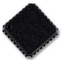
AD9649BCPZ-20 Analog Devices Inc, AD9649BCPZ-20 Datasheet - Page 26

AD9649BCPZ-20
Manufacturer Part Number
AD9649BCPZ-20
Description
IC ADC 14BIT 20MSPS 32LFCSP
Manufacturer
Analog Devices Inc
Datasheet
1.AD9649BCPZRL7-20.pdf
(32 pages)
Specifications of AD9649BCPZ-20
Data Interface
Serial, SPI™
Number Of Bits
14
Sampling Rate (per Second)
20M
Number Of Converters
1
Power Dissipation (max)
51.8mW
Voltage Supply Source
Analog and Digital
Operating Temperature
-40°C ~ 85°C
Mounting Type
Surface Mount
Package / Case
32-VFQFN, CSP Exposed Pad
Resolution (bits)
14bit
Sampling Rate
20MSPS
Input Channel Type
Differential
Supply Voltage Range - Analog
1.7V To 1.9V
Supply Voltage Range - Digital
1.7V To 3.6V
Lead Free Status / RoHS Status
Lead free / RoHS Compliant
Available stocks
Company
Part Number
Manufacturer
Quantity
Price
Company:
Part Number:
AD9649BCPZ-20
Manufacturer:
AD
Quantity:
3 100
AD9649
MEMORY MAP
READING THE MEMORY MAP REGISTER TABLE
Each row in the memory map register table (see Table 16) contains
eight bit locations. The memory map is roughly divided into four
sections: the chip configuration registers (Address 0x00 to
Address 0x02); the device transfer registers (Address 0xFF); the
program registers, including setup, control, and test (Address 0x08
to Address 0x2A); and the digital feature control registers
(Address 0x101).
Table 16 documents the default hexadecimal value for each
hexadecimal address shown. The column with the heading Bit 7
(MSB) is the start of the default hexadecimal value given. For
example, Address 0x2A, the OR/MODE select register, has a hexa-
decimal default value of 0x01. This means that in Address 0x2A,
Bits[7:1] = 0, and Bit 0 = 1. This setting is the default OR/MODE
setting. The default value results in the programmable external
MODE/OR pin (Pin 23) functioning as an out-of-range digital
output. For more information on this function and others, see the
AN-877 Application Note, Interfacing to High Speed ADCs via SPI.
This document details the functions controlled by Register 0x00
to Register 0xFF. The remaining register, Register 0x101, is docu-
mented in the Memory Map Register Descriptions section that
follows Table 16.
OPEN LOCATIONS
All address and bit locations that are not included in the SPI map
are not currently supported for this device. Unused bits of a valid
address location should be written with 0s. Writing to these loca-
tions is required only when part of an address location is open
(for example, Address 0x2A). If the entire address location is
open, it is omitted from the SPI map (for example, Address 0x13)
and should not be written.
Rev. 0 | Page 26 of 32
DEFAULT VALUES
After the AD9649 is reset, critical registers are loaded with default
values. The default values for the registers are given in the memory
map register table (see Table 16).
Logic Levels
An explanation of logic level terminology follows:
•
•
Transfer Register Map
Address 0x08 to Address 0x18 are shadowed. Writes to these
addresses do not affect part operation until a transfer command
is issued by writing 0x01 to Address 0xFF, setting the transfer bit.
This allows these registers to be updated internally and simulta-
neously when the transfer bit is set. The internal update takes
place when the transfer bit is set, and then the bit autoclears.
“Bit is set” is synonymous with “bit is set to Logic 1” or
“writing Logic 1 for the bit. ”
“Clear a bit” is synonymous with “bit is set to Logic 0” or
“writing Logic 0 for the bit. ”


