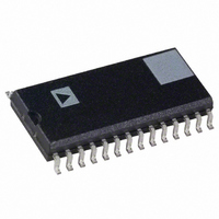
AD9221AR Analog Devices Inc, AD9221AR Datasheet - Page 5

AD9221AR
Manufacturer Part Number
AD9221AR
Description
IC ADC 12BIT 1.5MSPS 28-SOIC
Manufacturer
Analog Devices Inc
Datasheet
1.AD9220ARSZ-REEL.pdf
(32 pages)
Specifications of AD9221AR
Rohs Status
RoHS non-compliant
Number Of Bits
12
Sampling Rate (per Second)
1.5M
Data Interface
Parallel
Number Of Converters
7
Power Dissipation (max)
70mW
Voltage Supply Source
Single Supply
Operating Temperature
-40°C ~ 85°C
Mounting Type
Surface Mount
Package / Case
28-SOIC (0.300", 7.50mm Width)
For Use With
AD9221-EB - BOARD EVAL FOR AD9221
Available stocks
Company
Part Number
Manufacturer
Quantity
Price
Part Number:
AD9221AR
Manufacturer:
ADI/亚德诺
Quantity:
20 000
Part Number:
AD9221ARS
Manufacturer:
ADI/亚德诺
Quantity:
20 000
Part Number:
AD9221ARSZ
Manufacturer:
ADI/亚德诺
Quantity:
20 000
Part Number:
AD9221ARSZ-REEL
Manufacturer:
ADI/亚德诺
Quantity:
20 000
Part Number:
AD9221ARZ
Manufacturer:
ADI/亚德诺
Quantity:
20 000
Pin
Number
1
2
3–12
13
14
15, 26
16, 25
17
18
19
20
21
22
23
24
27
28
DEFINITIONS OF SPECIFICATIONS
Integral Nonlinearity (INL)
INL refers to the deviation of each individual code from a line
drawn from “negative full scale” through “positive full scale.”
The point used as negative full scale occurs 1/2 LSB before the
first code transition. Positive full scale is defined as a level 1 1/2
LSB beyond the last code transition. The deviation is measured
from the middle of each particular code to the true straight line.
Differential Nonlinearity (DNL, No Missing Codes)
An ideal ADC exhibits code transitions that are exactly 1 LSB
apart. DNL is the deviation from this ideal value. Guaranteed
no missing codes to 12-bit resolution indicates that all 4096
codes, respectively, must be present over all operating ranges.
REV. E
Mnemonic
CLK
BIT 12
BITS 11–2
BIT 1
OTR
AVDD
AVSS
SENSE
VREF
REFCOM
CAPB
CAPT
CML
VINA
VINB
DVSS
DVDD
PIN FUNCTION DESCRIPTIONS
(LSB) BIT 12
(MSB) BIT 1
PIN CONFIGURATION
BIT 11
BIT 10
BIT 9
BIT 8
BIT 7
BIT 6
BIT 5
BIT 4
BIT 3
BIT 2
OTR
CLK
10
11
12
13
14
1
2
3
4
5
6
7
8
9
Description
Clock Input Pin
Least Significant Data Bit (LSB)
Data Output Bit
Most Significant Data Bit (MSB)
Out of Range
5 V Analog Supply
Analog Ground
Reference Select
Reference I/O
Reference Common
Noise Reduction Pin
Noise Reduction Pin
Common-Mode Level (Midsupply)
Analog Input Pin (+)
Analog Input Pin (–)
Digital Ground
3 V to 5 V Digital Supply
(Not to Scale)
AD9221/
AD9223/
AD9220
TOP VIEW
28
27
26
25
24
23
22
21
20
19
18
17
16
15
DVDD
DVSS
AVDD
AVSS
VINB
VINA
CML
CAPT
CAPB
REFCOM
VREF
SENSE
AVSS
AVDD
–5–
Zero Error
The major carry transition should occur for an analog value 1/2
LSB below VINA = VINB. Zero error is defined as the devia-
tion of the actual transition from that point.
Gain Error
The first code transition should occur at an analog value 1/2 LSB
above negative full scale. The last transition should occur at an
analog value 1 1/2 LSB below the nominal full scale. Gain error
is the deviation of the actual difference between first and last
code transitions and the ideal difference between first and last
code transitions.
Temperature Drift
The temperature drift for zero error and gain error specifies the
maximum change from the initial (25°C) value to the value at
T
Power Supply Rejection
The specification shows the maximum change in full scale from
the value with the supply at the minimum limit to the value with
the supply at its maximum limit.
Aperture Jitter
Aperture jitter is the variation in aperture delay for successive
samples and is manifested as noise on the input to the A/D.
Aperture Delay
Aperture delay is a measure of the sample-and-hold amplifier
(SHA) performance and is measured from the rising edge of the
clock input to when the input signal is held for conversion.
Signal-to-Noise and Distortion (S/N+D, SINAD) Ratio
S/N+D is the ratio of the rms value of the measured input signal
to the rms sum of all other spectral components below the Nyquist
frequency, including harmonics but excluding dc. The value for
S/N+D is expressed in decibels.
Effective Number of Bits (ENOB)
For a sine wave, SINAD can be expressed in terms of the num-
ber of bits. Using the following formula,
it is possible to get a measure of performance expressed as N,
the effective number of bits.
Thus, effective number of bits for a device for sine wave inputs
at a given input frequency can be calculated directly from its
measured SINAD.
Total Harmonic Distortion (THD)
THD is the ratio of the rms sum of the first six harmonic com-
ponents to the rms value of the measured input signal and is
expressed as a percentage or in decibels.
Signal-to-Noise Ratio (SNR)
SNR is the ratio of the rms value of the measured input signal to
the rms sum of all other spectral components below the Nyquist
frequency, excluding the first six harmonics and dc. The value
for SNR is expressed in decibels.
Spurious Free Dynamic Range (SFDR)
SFDR is the difference in dB between the rms amplitude of the
input signal and the peak spurious signal.
MIN
or T
MAX
.
N
AD9221/AD9223/AD9220
=
(
SINAD
– .
1 76 6 02
)
/ .


