AD7821KRZ Analog Devices Inc, AD7821KRZ Datasheet
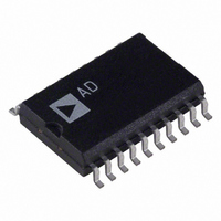
IC ADC 8BIT HS TRACK/HOLD 20SOIC

AD7821KRZ

Manufacturer Part Number
AD7821KRZ
Description
IC ADC 8BIT HS TRACK/HOLD 20SOIC
Manufacturer
Analog Devices Inc
Datasheet

Specifications of AD7821KRZ

Data Interface
Parallel
Number Of Bits
8
Sampling Rate (per Second)
1M
Number Of Converters
3
Power Dissipation (max)
50mW
Voltage Supply Source
Dual ±
Operating Temperature
-40°C ~ 85°C
Mounting Type
Surface Mount
Package / Case
20-SOIC (0.300", 7.50mm Width)
Resolution (bits)
8bit
Sampling Rate
1MSPS
Input Channel Type
Single Ended
Supply Voltage Range - Analog
4.75V To 5.25V
Supply Current
20mA
Digital Ic Case Style
SOIC
Lead Free Status / RoHS Status
Lead free / RoHS Compliant

Available stocks

Company
Part Number
Manufacturer
Quantity
Price
Part Number:
AD7821KRZ
Manufacturer:
TOSHIBA/东芝
Quantity:
20 000
a
GENERAL DESCRIPTION
The AD7821 is a high speed, 8-bit, sampling, analog-to-digital
converter that offers improved performance over the popular
AD7820. It offers a conversion time of 660 ns (versus 1.36 µs
for the AD7820) and 100 kHz signal bandwidth (versus 6.4
kHz). The sampling instant is better defined and occurs on the
falling edge of WR or RD. The provision of a V
allows the part to operate from ± 5 V supplies and to digitize
bipolar input signals. Alternatively, for unipolar inputs, the V
can be grounded and the AD7821 will operate from a single +5 V
supply, like the AD7820.
The AD7821 has a built-in track-and-hold function capable of
digitizing full-scale signals up to 100 kHz max. It also uses a
half-flash conversion technique that eliminates the need to gen-
erate a CLK signal for the ADC.
The AD7821 is designed with standard microprocessor control
signals (CS, RD, WR, RDY, INT) and latched, three-state data
outputs capable of interfacing to high speed data buses. An
overflow output (OFL) is also provided for cascading devices to
achieve higher resolution.
The AD7821 is fabricated in Linear Compatible CMOS
(LC
precision bipolar circuits with low power CMOS logic. The part
features a low power dissipation of 50 mW.
REV. B
Information furnished by Analog Devices is believed to be accurate and
reliable. However, no responsibility is assumed by Analog Devices for its
use, nor for any infringements of patents or other rights of third parties that
may result from its use. No license is granted by implication or otherwise
under any patent or patent rights of Analog Devices.
FEATURES
Fast Conversion Time: 660 ns Max
100 kHz Track-and-Hold Function
1 MHz Sample Rate
Unipolar and Bipolar Input Ranges
Ratiometric Reference Inputs
No External Clock
Extended Temperature Range Operation
Skinny 20-Lead DlPs, SOIC, and 20-Terminal
2
MOS), an advanced, mixed technology process combining
Surface-Mount Packages
SS
pin (Pin 19)
SS
LC
pin
8-Bit ADC with Track/Hold Function
2
MOS High Speed, P Compatible
PRODUCT HIGHLIGHTS
1. Fast Conversion Time
2. Built-In Track-and-Hold
3. Total Unadjusted Error
4. Unipolar/Bipolar Input Ranges
5. Dynamic Specifications for DSP Users
One Technology Way, P.O. Box 9106, Norwood, MA 02062-9106, U.S.A.
Tel: 781/329-4700
Fax: 781/326-8703
The half-flash conversion technique, coupled with fabrication
on Analog Devices’ LC
version time. The conversion time for the WR-RD mode is
660 ns, with 700 ns for the RD mode.
This allows input signals with slew rates up to 1.6 V/µs to be
converted to 8 bits without an external track-and-hold. This
corresponds to a 5 V peak-to-peak, 100 kHz sine wave signal.
The AD7821 features an excellent total unadjusted error figure
of less than ± 1 LSB over the full operating temperature range.
The AD7821 is specified for single-supply (+5 V) operation
with a unipolar full-scale range of 0 to +5 V, and for dual-supply
(±5 V) operation with a bipolar input range of ± 2.5 V. Typical
performance characteristics are given for other input ranges.
In addition to the traditional ADC specifications, the
AD7821 is specified for ac parameters, including signal-to-
noise ratio, distortion, and slew rate.
FUNCTIONAL BLOCK DIAGRAM
2
MOS process, enables a very fast con-
© Analog Devices, Inc., 2002
AD7821
www.analog.com

Related parts for AD7821KRZ

AD7821KRZ Summary of contents

Page 1

FEATURES Fast Conversion Time: 660 ns Max 100 kHz Track-and-Hold Function 1 MHz Sample Rate Unipolar and Bipolar Input Ranges Ratiometric Reference Inputs No External Clock Extended Temperature Range Operation Skinny 20-Lead DlPs, SOIC, and 20-Terminal Surface-Mount Packages GENERAL ...

Page 2

AD7821–SPECIFICATIONS V (–) = –2.5 V. These test conditions apply unless otherwise stated. All specifications T REF apply for RD Mode (Pin V). Parameter K Version UNIPOLAR INPUT RANGE 2 Resolution 8 ± Total Unadjusted ...

Page 3

TIMING CHARACTERISTICS Limit at Limit at + Parameter (All Versions) (K, B Versions CSS CSH RDY t 700 875 CRD 3 t ACC0 CRD ...

Page 4

AD7821 ABSOLUTE MAXIMUM RATINGS GND . . . . . . . . . . . . . . . . . . . . . . . . . . . –0 ...

Page 5

TERMINOLOGY LEAST SIGNIFICANT BIT (LSB) An ADC with 8-bit resolution can resolve one part full scale). For the AD7821 operating in either the unipolar or bipolar input range with 5 V full scale, one LSB is 19.53 ...

Page 6

Performance Characteristics AD7821 TPC 1. Conversion Time (RD Mode) vs.Temperature TPC 4. Accuracy vs TPC 7. Effective Number of Bits vs. Input Signal ( ± 2.5 V) Frequency TPC 2. Power Supply Current vs. Temperature (Not Including ...

Page 7

CIRCUIT INFORMATION BASIC DESCRIPTION The AD7821 uses a half flash conversion technique (see Func- tional Block Diagram), whereby two 4-bit flash ADCs are used to achieve an 8-bit result. Each 4-bit flash ADC contains 15 comparators, which compare an unknown ...

Page 8

AD7821 Figure 6. AD7821 Equivalent Input Circuit The input capacitors must charge to the input voltage through the on resistance of the analog switches (about 2 kΩ kΩ). In addition, about input stray capacitance must ...

Page 9

SIGNAL-TO-NOISE RATIO AND DISTORTION The dynamic performance of the AD7821 is evaluated by apply- ing a very low distortion sine wave signal to the analog input (V ) which is then sampled at a 512 kHz sampling rate. A Fast ...

Page 10

AD7821 RD Mode (MODE = 0) The timing diagram for the RD mode is shown in Figure 11. This mode is intended for use with microprocessors that have a WAIT state facility, whereby a READ instruction cycle can be extended ...

Page 11

MICROPROCESSOR INTERFACING The AD7821 is designed for easy interfacing to microprocessors as a memory mapped peripheral or an I/O device. This reduces to a minimum the amount of external logic required for interfacing. AD7821 – 68008 INTERFACE Figure 14 shows ...

Page 12

AD7821 APPLYING THE AD7821 The AD7821 is specified for a unipolar input range and a bipolar input range of –2 +2.5 V. The V V (+) voltages required for these input ranges ...

Page 13

Figure 21. 16-Channel Telecom ADC System SIMULTANEOUS SAMPLING ADC S The AD7821’s inherent track-and-hold and well defined sampling instant makes it useful in such applications as sonar, where a num- ber of input channels are required to be sampled simultaneously. ...

Page 14

AD7821 20-Lead Plastic Dual-in-Line Package [PDIP] (N-20) Dimensions shown in inches and (millimeters) 0.985 (25.02) 0.965 (24.51) 0.295 (7.49) 0.945 (24.00) 0.285 (7.24) 0.275 (6.99 0.180 (4.57) 0.015 (0.38) MIN MAX 0.150 (3.81) 0.130 (3.30) SEATING ...

Page 15

R Revision History Location 10/02—Data Sheet changed from REV REV. B. Update Format . . . . . . . . . . . . . ...

Page 16

–16– ...

Related keywords