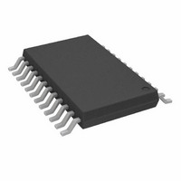
AD7714YRUZ Analog Devices Inc, AD7714YRUZ Datasheet - Page 16

AD7714YRUZ
Manufacturer Part Number
AD7714YRUZ
Description
IC ADC SIGNAL COND 3/5V 24-TSSOP
Manufacturer
Analog Devices Inc
Datasheet
1.AD7714YNZ.pdf
(40 pages)
Specifications of AD7714YRUZ
Data Interface
DSP, MICROWIRE™, QSPI™, Serial, SPI™
Number Of Bits
24
Sampling Rate (per Second)
1k
Number Of Converters
1
Power Dissipation (max)
7mW
Voltage Supply Source
Analog and Digital
Operating Temperature
-40°C ~ 105°C
Mounting Type
Surface Mount
Package / Case
24-TSSOP (0.173", 4.40mm Width)
Resolution (bits)
24bit
Sampling Rate
1kSPS
Input Channel Type
Differential
Supply Voltage Range - Digital
2.7V To 5.25V
Supply Current
1.1mA
Number Of Elements
1
Resolution
24Bit
Architecture
Delta-Sigma
Sample Rate
1KSPS
Input Polarity
Unipolar/Bipolar
Input Type
Voltage
Differential Input
Yes
Power Supply Requirement
Analog and Digital
Single Supply Voltage (typ)
3/5V
Single Supply Voltage (min)
2.7V
Single Supply Voltage (max)
5.25V
Dual Supply Voltage (typ)
Not RequiredV
Dual Supply Voltage (min)
Not RequiredV
Dual Supply Voltage (max)
Not RequiredV
Power Dissipation
4.75mW
Integral Nonlinearity Error
±0.0015%FSR
Operating Temp Range
-40C to 105C
Operating Temperature Classification
Industrial
Mounting
Surface Mount
Pin Count
24
Package Type
TSSOP
Lead Free Status / RoHS Status
Lead free / RoHS Compliant
For Use With
EVAL-AD7714-3EBZ - BOARD EVALUATION FOR AD7714
Lead Free Status / Rohs Status
Compliant
Available stocks
Company
Part Number
Manufacturer
Quantity
Price
Part Number:
AD7714YRUZ
Manufacturer:
ADI/亚德诺
Quantity:
20 000
AD7714
MD2
1
1
1
1
BO
FSYNC
MD1
0
0
1
1
MD0
0
1
0
1
Operating Mode (continued)
System-Offset Calibration; this activates system-offset calibration on the channel selected by CH2, CH1
and CH0 of the Communications Register. This is a one step calibration sequence and when complete
the part returns to Normal Mode with MD2, MD1 and MD0 returning to 0, 0, 0. The DRDY output
or bit goes high when calibration is initiated and returns low when this system offset calibration is com-
plete and a new valid word is available in the data register. For this calibration type, the zero-scale cali-
bration is performed at the selected gain on the input voltage provided at the analog input during this
calibration sequence. This input voltage should remain stable for the duration of the calibration. The
full-scale calibration is performed at the selected gain on an internally generated V
Background Calibration; this activates background calibration on the channel selected by CH2, CH1
and CH0 of the Communications Register. If the background calibration mode is on, then the AD7714
provides continuous self-calibration of the shorted (zeroed) inputs. This calibration takes place as part
of the conversion sequence, extending the conversion time and reducing the word rate by a factor of six.
Its major advantage is that the user does not have to worry about recalibrating the offset of the device
when there is a change in the ambient temperature or supplies. In this mode, the zero-scale calibration
is performed at the selected gain on internally shorted (zeroed) inputs. The calibrations are interleaved
with normal conversions and the calibration registers of the device are automatically updated. Because
the background calibration does not perform full-scale calibrations, a self-calibration should be per-
formed before placing the part in the background calibration mode.
Zero-Scale Self-Calibration; this activates zero-scale self-calibration on the channel selected by CH2,
CH1 and CH0 of the Communications Register. This zero-scale self-calibration is performed at the
selected gain on internally shorted (zeroed) inputs. This is a one step calibration sequence and when
complete the part returns to Normal Mode with MD2, MD1 and MD0 returning to 0, 0, 0. The DRDY
output or bit goes high when calibration is initiated and returns low when this zero-scale self-calibration
is complete and a new valid word is available in the data register.
Full-Scale Self-Calibration; this activates full-scale self-calibration on the channel selected by CH2,
CH1 and CH0 of the Communications Register. This full-scale self-calibration is performed at the
selected gain on an internally-generated V
when complete the part returns to Normal Mode with MD2, MD1 and MD0 returning to 0, 0, 0. The
DRDY output or bit goes high when calibration is initiated and returns low when this full-scale self-
calibration is complete and a new valid word is available in the data register.
G2
0
0
0
0
1
1
1
1
Burnout Current. A 0 in this bit turns off the on-chip burnout currents. This is the default (Power-On
or RESET) status of this bit. A 1 in this bit activates the burnout currents. When active, the burnout
currents connect to the selected analog input pair, one to the AIN(+) input and one to the AIN(–) input.
Filter Synchronization. When this bit is high, the nodes of the digital filter, the filter control logic and
the calibration control logic are held in a reset state and the analog modulator is also held in its reset
state. When this bit goes low, the modulator and filter start to process data and a valid word is available
in 3
digital interface and does not reset the DRDY output if it is low.
1/(output update rate), i.e., the settling time of the filter. This FSYNC bit does not affect the
G1
0
0
1
1
0
0
1
1
G0
0
1
0
1
0
1
0
1
Gain Setting
1
2
4
8
16
32
64
128
–16–
REF
/Selected Gain. This is a one step calibration sequence and
REF
/Selected Gain.
REV. C


