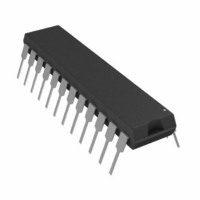
AD7714YN Analog Devices Inc, AD7714YN Datasheet - Page 20

AD7714YN
Manufacturer Part Number
AD7714YN
Description
IC ADC 24BIT SIGMA-DELTA 24-DIP
Manufacturer
Analog Devices Inc
Datasheet
1.AD7714YNZ.pdf
(40 pages)
Specifications of AD7714YN
Rohs Status
RoHS non-compliant
Number Of Bits
24
Sampling Rate (per Second)
1k
Data Interface
DSP, MICROWIRE™, QSPI™, Serial, SPI™
Number Of Converters
1
Power Dissipation (max)
7mW
Voltage Supply Source
Analog and Digital
Operating Temperature
-40°C ~ 105°C
Mounting Type
Through Hole
Package / Case
24-DIP (0.300", 7.62mm)
For Use With
EVAL-AD7714-3EBZ - BOARD EVALUATION FOR AD7714
Available stocks
Company
Part Number
Manufacturer
Quantity
Price
AD7714
ANALOG INPUT
Analog Input Ranges
The AD7714 contains six analog input pins (labelled AIN1 to
AIN6) which can be configured as either three fully differential
input channels or five pseudo-differential input channels. Bits
CH0, CH1 and CH2 of the Communications Register configure
the analog input arrangement and the channel selection is as
outlined previously in Table VII. The input pairs (either differ-
ential or pseudo-differential) provide programmable-gain, input
channels which can handle either unipolar or bipolar input
signals. It should be noted that the bipolar input signals are
referenced to the respective AIN(–) input of the input pair.
In unbuffered mode, the common-mode range of these inputs is
from AGND to AV
input voltage lies between AGND – 30 mV and AV
This means that in unbuffered mode the part can handle both
unipolar and bipolar input ranges for all gains. In buffered
mode, the analog inputs can handle much larger source imped-
ances, but the absolute input voltage range is restricted to be-
tween AGND + 50 mV to AV
restrictions on the common-mode range. This means that in
buffered mode there are some restrictions on the allowable gains
for bipolar input ranges. Care must be taken in setting up the
common-mode voltage and input voltage range so that the
above limits are not exceeded, otherwise there will be a degrada-
tion in linearity performance.
In unbuffered mode, the analog inputs look directly into the
7 pF input sampling capacitor, C
current in this unbuffered mode is 1 nA maximum. As a result,
the analog inputs see a dynamic load which is switched at the
input sample rate (see Figure 3). This sample rate depends on
master clock frequency and selected gain. C
AIN(+) and discharged to AIN(–) every input sample cycle.
The effective on-resistance of the switch, R
AIN(+)
AIN(–)
Figure 3. Unbuffered Analog Input Structure
SWITCHING FREQUENCY DEPENDS ON
f
CLKIN
AND SELECTED GAIN
DD
provided that the absolute value of the analog
R
SW
(7k
DD
C
(7pF )
SAMP
SAMP
– 1.5 V which also places
TYP)
V
BIAS
. The dc input leakage
SW
HIGH
IMPEDANCE
>1G
SAMP
, is typically 7 k .
is charged to
DD
+ 30 mV.
–20–
C
source impedances every input sample cycle. Therefore, in unbuf-
fered mode, source impedances mean a longer charge time for
C
shows the allowable external resistance/capacitance values, for
unbuffered mode, such that no gain error to the 16-bit level is
introduced on the part. Table XIII shows the allowable external
resistance/capacitance values, once again for unbuffered mode,
such that no gain error to the 20-bit level is introduced.
Gain
1
2
4
8–128 35.2 k
Gain
1
2
4
8–128 26.8 k
In buffered mode, the analog inputs look into the high impedance
inputs stage of the on-chip buffer amplifier. C
this buffer amplifier such that source impedances do not affect
the charging of C
age current of 1 nA. In this buffered mode, large source imped-
ances result in a dc offset voltage developed across the source
impedance but not in a gain error.
Input Sample Rate
The modulator sample frequency for the AD7714 remains at
f
the selected gain. However, gains greater than 1 are achieved
by a combination of multiple input samples per modulator cycle
and a scaling of the ratio of reference capacitor to input capaci-
tor. As a result of the multiple sampling, the input sample rate
of the device varies with the selected gain (see Table XIV). In
buffered mode, the input is buffered before the input sampling
capacitor. In unbuffered mode, where the analog input looks
directly into the sampling capacitor, the effective input imped-
ance is 1/C
tance and f
CLK IN
SAMP
SAMP
Table XII. External R, C Combination for No 16-Bit Gain
Error (Unbuffered Mode Only)
Table XIII. External R, C Combination for No 20-Bit Gain
Error (Unbuffered Mode Only)
/128 (19.2 kHz @ f
must be charged through R
and this may result in gain errors on the part. Table XII
0
368 k
177.2 k
82.8 k
0
290 k
141 k
63.6 k
SAMP
S
is the input sample rate.
SAMP
50
90.6 k
44.2 k
21.2 k
9.6 k
f
50
69 k
33.8 k
16 k
7.2 k
S
External Capacitance (pF)
where C
External Capacitance (pF)
. This buffer amplifier has an offset leak-
CLK IN
100
54.2 k
5.8 k
26.4 k
12.6 k
100
40.8 k
20 k
9.6 k
4.4 k
SAMP
= 2.4576 MHz) regardless of
SW
is the input sampling capaci-
500
14.6 k
7.2 k
3.4 k
1.58 k
and through any external
500
10.4 k
5 k
2.4 k
1.1 k
SAMP
1000
8.2 k
4 k
1.94 k
880
1000
5.6 k
2.8 k
1.34 k
600
is charged via
5000
2.2 k
1.12 k
540
240
REV. C
5000
1.4 k
700
340
160


