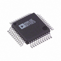
AD7859ASZ Analog Devices Inc, AD7859ASZ Datasheet - Page 4

AD7859ASZ
Manufacturer Part Number
AD7859ASZ
Description
IC ADC 12BIT 8CH LP 44-MQFP
Manufacturer
Analog Devices Inc
Datasheet
1.AD7859LASZ.pdf
(28 pages)
Specifications of AD7859ASZ
Data Interface
Parallel
Number Of Bits
12
Sampling Rate (per Second)
200k
Number Of Converters
2
Power Dissipation (max)
30mW
Voltage Supply Source
Analog and Digital
Operating Temperature
-40°C ~ 85°C
Mounting Type
Surface Mount
Package / Case
44-MQFP, 44-PQFP
Resolution (bits)
12bit
Sampling Rate
100kSPS
Input Channel Type
Single Ended
Supply Voltage Range - Analog
3V To 5.5V
Supply Voltage Range - Digital
3V To 5.5V
Lead Free Status / RoHS Status
Lead free / RoHS Compliant
Available stocks
Company
Part Number
Manufacturer
Quantity
Price
Company:
Part Number:
AD7859ASZ
Manufacturer:
Analog Devices Inc
Quantity:
10 000
Part Number:
AD7859ASZ
Manufacturer:
ADI/亚德诺
Quantity:
20 000
Company:
Part Number:
AD7859ASZ-REEL
Manufacturer:
Analog Devices Inc
Quantity:
10 000
AD7859/AD7859L
TIMING SPECIFICATIONS
Parameter
f
t
t
t
t
t
t
t
t
t
t
t
t
t
t
t
t
t
t
t
t
t
t
t
NOTES
1
2
3
4
5
6
Specifications subject to change without notice.
CLKIN
1
2
CONVERT
3
4
5
6
7
8
9
10
11
12
13
14
15
16
17
19
CAL
CAL1
CAL2
Sample tested at +25 C to ensure compliance. All input signals are specified with tr = tf = 5 ns (10% to 90% of V
Mark/Space ratio for the master clock input is 40/60 to 60/40.
The CONVST pulse width will here only apply for normal operation. When the part is in power-down mode, a different CONVST pulse width will apply (see Power-
Down section).
Measured with the load circuit of Figure 1 and defined as the time required for the output to cross 0.8 V or 2.4 V.
t
back to remove the effects of charging or discharging the 50 pF capacitor. This means that the time, t
time of the part and is independent of the bus loading.
The typical time specified for the calibration times is for a master clock of 4 MHz. For the L version the calibration times will be longer than those quoted here due to
the 1.8 MHz master clock.
18
9
3
4
5
4
is derived form the measured time taken by the data outputs to change 0.5 V when loaded with the circuit of Figure 1. The measured number is then extrapolated
6
6
6
2
5 V
500
4
1.8
100
50
4.5
10
15
5
0
0
55
50
5
40
60
0
5
0
0
55
10
5
1/2 t
2.5 t
31.25
27.78
3.47
CLKIN
CLKIN
Limit at T
(A, B Versions)
MIN
3 V
500
4
1.8
100
90
4.5
10
15
5
0
0
55
50
5
40
70
0
5
0
0
70
10
5
1/2 t
2.5 t
31.25
27.78
3.47
, T
1
MAX
(AV
T
CLKIN
CLKIN
A
= T
DD
= DV
MIN
to T
DD
= +3.0 V to +5.5 V; f
MAX
Units
kHz min
MHz max
MHz max
ns min
ns max
ns min
ns min
ns min
ns min
ns min
ns max
ns min
ns max
ns min
ns min
ns max
ns min
ns max
ns min
ns min
ns min
ns min
ns max
ms typ
ms typ
ms typ
s max
s max
, unless otherwise noted)
–4–
Description
Master Clock Frequency
L Version
CONVST Pulse Width
CONVST to BUSY
HBEN to RD Setup Time
HBEN to RD Hold Time
CS to RD to Setup Time
CS to RD Hold Time
RD Pulse Width
CS to WR Setup Time
CS to WR Hold Time
WR Pulse Width
Data Setup Time Before WR
Data Hold Time After WR
Full Self-Calibration Time, Master Clock Dependent (125013
t
Internal DAC Plus System Full-Scale Cal Time, Master Clock
Dependent (111124 t
System Offset Calibration Time, Master Clock Dependent
(13889 t
Conversion Time = 18 t
L Version 1.8 MHz CLKIN. Conversion Time = 18 t
Data Access Time After RD
Bus Relinquish Time After RD
Bus Relinquish Time After RD
Minimum Time Between Reads
HBEN to WR Setup Time
HBEN to WR Hold Time
New Data Valid Before Falling Edge of BUSY
CS
CLKIN
CLKIN
to BUSY
)
= 4 MHz for AD7859 and 1.8 MHz for AD7859L;
CLKIN
)
9
, quoted in the timing characteristics is the true bus relinquish
in Calibration Sequence
CLKIN
Propagation Delay
DD
CLKIN
) and timed from a voltage level of 1.6 V.
)
CLKIN
REV. A


