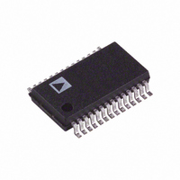
AD9201ARS Analog Devices Inc, AD9201ARS Datasheet - Page 2

AD9201ARS
Manufacturer Part Number
AD9201ARS
Description
IC ADC CMOS 10BIT DUAL 28-SSOP
Manufacturer
Analog Devices Inc
Specifications of AD9201ARS
Mounting Type
Surface Mount
Rohs Status
RoHS non-compliant
Number Of Bits
10
Sampling Rate (per Second)
20M
Data Interface
Parallel
Number Of Converters
2
Power Dissipation (max)
245mW
Voltage Supply Source
Analog and Digital
Operating Temperature
-40°C ~ 85°C
Package / Case
28-SSOP (0.200", 5.30mm Width)
Input Channels Per Adc
2
No. Of Channels
2
Peak Reflow Compatible (260 C)
No
Inl ±
2.5LSB
Sample Rate
20MSPS
No. Of Bits
10 Bit
Leaded Process Compatible
No
Dnl±
1LSB
Number Of Elements
2
Resolution
10Bit
Architecture
Pipelined
Input Polarity
Unipolar
Input Type
Voltage
Rated Input Volt
1.5V
Differential Input
Yes
Power Supply Requirement
Analog and Digital
Single Supply Voltage (typ)
3V
Single Supply Voltage (min)
2.7V
Single Supply Voltage (max)
5.5V
Dual Supply Voltage (typ)
Not RequiredV
Dual Supply Voltage (min)
Not RequiredV
Dual Supply Voltage (max)
Not RequiredV
Differential Linearity Error
±1LSB
Integral Nonlinearity Error
±2.5LSB
Operating Temp Range
-40C to 85C
Operating Temperature Classification
Industrial
Mounting
Surface Mount
Pin Count
28
Package Type
SSOP
Lead Free Status / Rohs Status
Not Compliant
Available stocks
Company
Part Number
Manufacturer
Quantity
Price
Part Number:
AD9201ARS
Manufacturer:
ADI/亚德诺
Quantity:
20 000
Part Number:
AD9201ARSZ
Manufacturer:
ADI/亚德诺
Quantity:
20 000
Company:
Part Number:
AD9201ARSZ-REEL
Manufacturer:
SIEMENS
Quantity:
3
Parameter
RESOLUTION
CONVERSION RATE
DC ACCURACY
ANALOG INPUT
INTERNAL REFERENCE
POWER SUPPLY
DYNAMIC PERFORMANCE
AD9201–SPECIFICATIONS
Differential Nonlinearity
Integral Nonlinearity
Differential Nonlinearity (SE)
Integral Nonlinearity (SE)
Zero-Scale Error, Offset Error
Full-Scale Error, Gain Error
Gain Match
Offset Match
Input Voltage Range
Input Capacitance
Aperture Delay
Aperture Uncertainty (Jitter)
Aperture Delay Match
Input Bandwidth (–3 dB)
Output Voltage (1 V Mode)
Output Voltage Tolerance (1 V Mode)
Output Voltage (2 V Mode)
Output Voltage Tolerance (2 V Mode)
Load Regulation (1 V Mode)
Load Regulation (2 V Mode)
Operating Voltage
Supply Current
Power Consumption
Power-Down
Power Supply Rejection
Signal-to-Noise and Distortion
Signal-to-Noise
Total Harmonic Distortion
Spurious Free Dynamic Range
Two-Tone Intermodulation Distortion
Differential Phase
Differential Gain
Crosstalk Rejection
Small Signal (–20 dB)
Full Power (0 dB)
f = 3.58 MHz
f = 10 MHz
f = 3.58 MHz
f = 10 MHz
f = 3.58 MHz
f = 10 MHz
f = 3.58 MHz
f = 10 MHz
1
2
Symbol
F
DNL
INL
DNL
INL
E
E
AIN
C
t
t
BW
VREF
VREF
AVDD
DRVDD
I
I
P
PSR
SINAD
SNR
THD
SFDR
IMD
DP
DG
AP
AJ
AVDD
DRVDD
D
S
ZS
FS
IN
(AVDD = +3 V, DVDD = +3 V, F
internal ref, differential input signal, unless otherwise noted)
Min
–0.5
2.7
2.7
55.6
55.9
–66
–2–
Typ
10
1.2
2
4
2
2
240
245
1
2
3
3
71.6
0.1
215
15.5
0.8
57.3
55.8
57.8
56.2
–69
–66.3
–73
–70.5
–62
0.1
0.05
68
0.4
0.5
1.5
1.5
3.5
0.5
5
10
15
15
Max
20
AVDD/2
5.5
5.5
245
1.3
–63.3
1
2.5
3.8
5.4
28
SAMPLE
mW
Units
Bits
MHz
LSB
LSB
LSB
LSB
% FS
% FS
LSB
LSB
V
pF
ns
ps
ps
MHz
MHz
V
mV
V
mV
mV
mV
V
V
mA
mA
mW
% FS
dB
dB
dB
dB
dB
dB
dB
dB
dB
Degree
%
dB
= 20 MSPS, VREF = 2 V, INB = 0.5 V, T
REFT = 1 V, REFB = 0 V
REFT = 1 V, REFB = 0 V
REFSENSE = VREF
REFSENSE = GND
1 mA Load Current
1 mA Load Current
AVDD – DVDD 2.3 V
AVDD = 3 V
AVDD = DVDD = 3 V
STBY = AVDD, Clock = AVSS
f = 44.49 MHz and 45.52 MHz
NTSC 40 IRE Mod Ramp
Condition
F
S
= 14.3 MHz
MIN
REV. D
to T
MAX,


