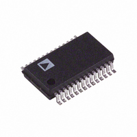
AD9200ARSRL Analog Devices Inc, AD9200ARSRL Datasheet - Page 2

AD9200ARSRL
Manufacturer Part Number
AD9200ARSRL
Description
IC ADC 10BIT CMOS 20MSPS 28-SSOP
Manufacturer
Analog Devices Inc
Datasheet
1.AD9200ARSZRL.pdf
(24 pages)
Specifications of AD9200ARSRL
Rohs Status
RoHS non-compliant
Number Of Bits
10
Sampling Rate (per Second)
20M
Data Interface
Parallel
Number Of Converters
9
Power Dissipation (max)
100mW
Voltage Supply Source
Single Supply
Operating Temperature
-40°C ~ 85°C
Mounting Type
Surface Mount
Package / Case
28-SSOP (0.200", 5.30mm Width)
Parameter
RESOLUTION
CONVERSION RATE
DC ACCURACY
REFERENCE VOLTAGES
ANALOG INPUT
INTERNAL REFERENCE
POWER SUPPLY
DYNAMIC PERFORMANCE (AIN = 0.5 dBFS)
AD9200–SPECIFICATIONS
Differential Nonlinearity
Integral Nonlinearity
Offset Error
Gain Error
Top Reference Voltage
Bottom Reference Voltage
Differential Reference Voltage
Reference Input Resistance
Input Voltage Range
Input Capacitance
Aperture Delay
Aperture Uncertainty (Jitter)
Input Bandwidth (–3 dB)
DC Leakage Current
Output Voltage (1 V Mode)
Output Voltage Tolerance (1 V Mode)
Output Voltage (2 V Mode)
Load Regulation (1 V Mode)
Operating Voltage
Supply Current
Power Consumption
Power-Down
Gain Error Power Supply Rejection
Signal-to-Noise and Distortion
Effective Bits
Signal-to-Noise
Total Harmonic Distortion
Spurious Free Dynamic Range
Two-Tone Intermodulation
Differential Phase
Differential Gain
Full Power (0 dB)
f = 3.58 MHz
f = 10 MHz
f = 3.58 MHz
f = 10 MHz
f = 3.58 MHz
f = 10 MHz
f = 3.58 MHz
f = 10 MHz
f = 3.58 MHz
f = 10 MHz
Distortion
1
Symbol Min
F
DNL
INL
E
E
REFTS
REFBS
AIN
C
t
t
BW
VREF
VREF
AVDD
DRVDD 2.7
IAVDD
P
PSRR
SINAD
SNR
THD
SFDR
IMD
DP
DG
AJ
AP
S
ZS
FS
D
IN
1
GND
REFBS
2.7
54.5
55
–59
–61
(AVDD = +3 V, DRVDD = +3 V, F
Span from 0.5 V to 2.5 V, External Reference, T
Typ
10
0.4
1.4
2
10
4.2
1
4
2
300
23
1
2
0.5
3
3
26.6
80
4
1
57
54
9.1
8.6
57
56
–66
–58
–69
–61
68
0.1
0.05
0.5
0.75
10
–2–
Max
20
1.2
3.5
AVDD
AVDD – 1 V
REFTS
2
5.5
5.5
33.3
100
1
2
25
Units
Bits
MHz
LSB
LSB
% FSR
% FSR
V
V p-p
k
k
V
pF
ns
ps
MHz
V
mV
V
mV
V
V
mA
mW
mW
% FS
dB
dB
Bits
Bits
dB
dB
dB
dB
dB
dB
dB
Degree
%
A
S
= 20 MHz (50% Duty Cycle), MODE = AVDD, 2 V Input
Condition
REFTS = 2.5 V, REFBS = 0.5 V
REFTS, REFBS: MODE = AVDD
Between REFTF and REFBF: MODE = AVSS
REFBS Min = GND: REFTS Max = AVDD
Switched
Input = FS
REFSENSE = VREF
REFSENSE = GND
1 mA Load Current
AVDD = 3 V, MODE = AVSS
AVDD = DRVDD = 3 V, MODE = AVSS
STBY = AVDD, MODE and CLOCK =
AVSS
f = 44.49 MHz and 45.52 MHz
NTSC 40 IRE Mod Ramp
MIN
to T
MAX
unless otherwise noted)
REV. E


