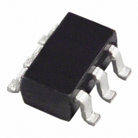
AD7466BRTZ-R2 Analog Devices Inc, AD7466BRTZ-R2 Datasheet - Page 24

AD7466BRTZ-R2
Manufacturer Part Number
AD7466BRTZ-R2
Description
IC ADC 12BIT 1.6V LP SOT23-6
Manufacturer
Analog Devices Inc
Specifications of AD7466BRTZ-R2
Data Interface
DSP, MICROWIRE™, QSPI™, Serial, SPI™
Design Resources
Software Calibrated, 50 MHz to 9 GHz, RF Power Measurement System (CN0178)
Number Of Bits
12
Sampling Rate (per Second)
200k
Number Of Converters
1
Power Dissipation (max)
900µW
Voltage Supply Source
Single Supply
Operating Temperature
-40°C ~ 85°C
Mounting Type
Surface Mount
Package / Case
SOT-23-6
Resolution (bits)
12bit
Sampling Rate
200kSPS
Input Channel Type
Single Ended
Supply Voltage Range - Analog
1.6V To 3.6V
Supply Current
300µA
Lead Free Status / RoHS Status
Lead free / RoHS Compliant
For Use With
EVAL-AD7466CBZ - BOARD EVALUATION FOR AD7466
Lead Free Status / RoHS Status
Lead free / RoHS Compliant, Lead free / RoHS Compliant
Available stocks
Company
Part Number
Manufacturer
Quantity
Price
Part Number:
AD7466BRTZ-R2
Manufacturer:
ADI/亚德诺
Quantity:
20 000
AD7466/AD7467/AD7468
The connection diagram in Figure 33 shows how the ADSP-218x
has the TFS and RFS of the SPORT tied together, with TFS set
as an output and RFS set as an input. The DSP operates in
alternate framing mode, and the SPORT control register is set
up as described. The frame synchronization signal generated on
the TFS is tied to CS , and as with all signal processing applica-
tions, equidistant sampling is necessary. However, in this example,
the timer interrupt is used to control the sampling rate of the
ADC and, under certain conditions, equidistant sampling might
not be achieved.
The timer registers, for example, are loaded with a value that
provides an interrupt at the required sample interval. When an
interrupt is received, a value is transmitted with TFS/DT (ADC
control word). The TFS is used to control the RFS and, there-
fore, the reading of data. The frequency of the serial clock is set
in the SCLKDIV register. When the instruction to transmit with
TFS is given (that is, AX0 = TX0), the state of the SCLK is
checked. The DSP waits until the SCLK goes high, low, and high
again before transmission starts. If the timer and SCLK values
are chosen such that the instruction to transmit occurs on or
near the rising edge of SCLK, the data can be transmitted, or it
can wait until the next clock edge.
For example, the ADSP-2181 has a master clock frequency of
16 MHz. If the SCLKDIV register is loaded with the value 3, an
SCLK of 2 MHz is obtained, and eight master clock periods
elapse for every SCLK period. If the timer registers are loaded
with the value 803, 100.5 SCLKs occur between interrupts and,
subsequently, between transmit instructions. This situation
results in nonequidistant sampling as the transmit instruction is
occurring on an SCLK edge. If the number of SCLKs between
interrupts is a whole integer figure of N, equidistant sampling is
implemented by the DSP.
1
ADDITIONAL PINS OMITTED FOR CLARITY.
AD7466/
AD7467/
AD7468
Figure 33. Interfacing to the ADSP-218x
SDATA
1
SCLK
CS
SCLK
DR
RFS
TFS
ADSP-218x
1
Rev. C | Page 24 of 28
AD7466/AD7467/AD7468 to DSP563xx Interface
The connection diagram in Figure 34 shows how the AD7466/
AD7467/AD7468 can be connected to the synchronous serial
interface (SSI) of the DSP563xx family of DSPs from Motorola.
The SSI is operated in synchronous mode and normal mode
(SYN = 1 and MOD = 0 in Control Register B, CRB) with an
internally generated word frame sync for both Tx and Rx
(Bit FSL1 = 0 and Bit FSL0 = 0 in the CRB register). Set the
word length in Control Register A (CRA) to 16 by setting Bits
WL2 = 0, WL1 = 1, and WL0 = 0 for the AD7466. The word
length for the AD7468 can be set to 12 bits (WL2 = 0, WL1 = 0,
and WL0 = 1). This DSP does not offer the option for a 14-bit
word length, so the AD7467 word length is set up to 16 bits like
the AD7466 word length. In this case, the user should keep in
mind that the last two bits are invalid data because the SDATA
goes back into three-state on the 14th SCLK falling edge.
The frame sync polarity bit (FSP) in the CRB register can be set
to 1, which means the frame goes low and a conversion starts.
Likewise, by means of Bits SCD2, SCKD, and SHFD in the CRB
register, it is established that Pin SC2 (the frame sync signal)
and Pin SCK in the serial port are configured as outputs, and
the most significant bit (MSB) is shifted first. To summarize,
MOD = 0
SYN = 1
WL2, WL1, WL0 depend on the word length
FSL1 = 0, FSL0 = 0
FSP = 1, negative frame sync
SCD2 = 1
SCKD = 1
SHFD = 0
For signal processing applications, it is imperative that the
frame synchronization signal from the DSP563xx provides
equidistant sampling.
1
ADDITIONAL PINS OMITTED FOR CLARITY.
AD7468
AD7466/
AD7467/
Figure 34. Interfacing to the DSP563xx
SDATA
1
SCLK
CS
SCK
SRD
SC2
DSP563xx
1


