AD7466BRTZ-R2 Analog Devices Inc, AD7466BRTZ-R2 Datasheet - Page 11
AD7466BRTZ-R2
Manufacturer Part Number
AD7466BRTZ-R2
Description
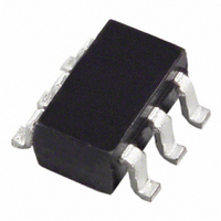
IC ADC 12BIT 1.6V LP SOT23-6
Manufacturer
Analog Devices Inc
Specifications of AD7466BRTZ-R2
Data Interface
DSP, MICROWIRE™, QSPI™, Serial, SPI™
Design Resources
Software Calibrated, 50 MHz to 9 GHz, RF Power Measurement System (CN0178)
Number Of Bits
12
Sampling Rate (per Second)
200k
Number Of Converters
1
Power Dissipation (max)
900µW
Voltage Supply Source
Single Supply
Operating Temperature
-40°C ~ 85°C
Mounting Type
Surface Mount
Package / Case
SOT-23-6
Resolution (bits)
12bit
Sampling Rate
200kSPS
Input Channel Type
Single Ended
Supply Voltage Range - Analog
1.6V To 3.6V
Supply Current
300µA
Lead Free Status / RoHS Status
Lead free / RoHS Compliant
For Use With
EVAL-AD7466CBZ - BOARD EVALUATION FOR AD7466
Lead Free Status / RoHS Status
Lead free / RoHS Compliant, Lead free / RoHS Compliant
Available stocks
Company
Part Number
Manufacturer
Quantity
Price

Part Number:
AD7466BRTZ-R2
Manufacturer:
ADI/亚德诺
Quantity:
20 000


ABSOLUTE MAXIMUM RATINGS
T
100 mA do not cause SCR latch-up.
Table 5.
Parameter
V
Analog Input Voltage to GND
Digital Input Voltage to GND
Digital Output Voltage to GND
Input Current to any Pin Except Supplies
Operating Temperature Range
SOT-23 Package
MSOP Package
Lead Temperature, Soldering
ESD
ESD CAUTION
ESD (electrostatic discharge) sensitive device. Electrostatic charges as high as 4000 V readily accumulate on
the human body and test equipment and can discharge without detection. Although this product features
proprietary ESD protection circuitry, permanent damage may occur on devices subjected to high energy
electrostatic discharges. Therefore, proper ESD precautions are recommended to avoid performance
degradation or loss of functionality.
DD
A
Commercial (B Version)
Storage Temperature Range
Junction Temperature
θ
θ
θ
θ
Vapor Phase (60 sec)
Infared (15 sec)
= 25°C, unless otherwise noted. Transient currents of up to
JA
JC
JA
JC
to GND
Thermal Impedance
Thermal Impedance
Thermal Impedance
Thermal Impedance
Rating
−0.3 V to +7 V
−0.3 V to V
−0.3 V to +7 V
−0.3 V to V
±10 mA
−40°C to +85°C
−65°C to +150°C
150°C
229.6°C/W
91.99°C/W
205.9°C/W
43.74°C/W
215°C
220°C
3.5 kV
DD
DD
+ 0.3 V
+ 0.3 V
Rev. B | Page 11 of 28
Stresses above those listed under Absolute Maximum Ratings
may cause permanent damage to the device. This is a stress
rating only; functional operation of the device at these or any
other conditions above those indicated in the operational
section of this specification is not implied. Exposure to absolute
maximum rating conditions for extended periods may affect
device reliability.
AD7466/AD7467/AD7468
Related parts for AD7466BRTZ-R2
Image
Part Number
Description
Manufacturer
Datasheet
Request
R

Part Number:
Description:
Dual Precision, 500 ns Settling, BiFET Op Amp
Manufacturer:
Analog Devices
Datasheet:

Part Number:
Description:
±1.7g Dual-Axis IMEMS Accelerometer Evaluation Board
Manufacturer:
Analog Devices Inc
Datasheet:

Part Number:
Description:
Inertial Sensor Evaluation System
Manufacturer:
Analog Devices Inc
Datasheet:
Part Number:
Description:
Manufacturer:
Analog Devices Inc
Datasheet:
Part Number:
Description:
Manufacturer:
Analog Devices Inc
Datasheet:
Part Number:
Description:
Manufacturer:
Analog Devices Inc
Datasheet:
Part Number:
Description:
Manufacturer:
Analog Devices Inc
Datasheet:
Part Number:
Description:
Manufacturer:
Analog Devices Inc
Datasheet:
Part Number:
Description:
Manufacturer:
Analog Devices Inc
Datasheet:
Part Number:
Description:
Manufacturer:
Analog Devices Inc
Datasheet:
Part Number:
Description:
Manufacturer:
Analog Devices Inc
Datasheet:
Part Number:
Description:
Manufacturer:
Analog Devices Inc
Datasheet:
Part Number:
Description:
Manufacturer:
Analog Devices Inc
Datasheet: