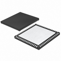
LTC2220IUP#TRPBF Linear Technology, LTC2220IUP#TRPBF Datasheet - Page 22

LTC2220IUP#TRPBF
Manufacturer Part Number
LTC2220IUP#TRPBF
Description
IC ADC 12BIT 170MSPS 64-QFN
Manufacturer
Linear Technology
Datasheet
1.LTC2220CUPPBF.pdf
(32 pages)
Specifications of LTC2220IUP#TRPBF
Number Of Bits
12
Sampling Rate (per Second)
170M
Data Interface
Parallel
Number Of Converters
1
Power Dissipation (max)
1.18W
Voltage Supply Source
Single Supply
Operating Temperature
-40°C ~ 85°C
Mounting Type
Surface Mount
Package / Case
64-WFQFN, Exposed Pad
Lead Free Status / RoHS Status
Lead free / RoHS Compliant
Available stocks
Company
Part Number
Manufacturer
Quantity
Price
LTC2220/LTC2221
Other voltage ranges in between the pin selectable ranges
can be programmed with two external resistors as shown
in Figure 10. An external reference can be used by applying
its output directly or through a resistor divider to SENSE.
It is not recommended to drive the SENSE pin with a logic
device. The SENSE pin should be tied to the appropriate
level as close to the converter as possible. If the SENSE pin
is driven externally, it should be bypassed to ground as
close to the device as possible with a 1µF ceramic capacitor.
Input Range
The input range can be set based on the application. The
2V input range will provide the best signal-to-noise perfor-
mance while maintaining excellent SFDR. The 1V input
range will have better SFDR performance, but the SNR will
degrade by 5dB. See the Typical Performance Character-
istics section.
Driving the Encode Inputs
The noise performance of the LTC2220/LTC2221 can
depend on the encode signal quality as much as on the
analog input. The ENC
driven differentially, primarily for noise immunity from
common mode noise sources. Each input is biased through
a 6k resistor to a 1.6V bias. The bias resistors set the DC
operating point for transformer coupled drive circuits and
can set the logic threshold for single-ended drive circuits.
Any noise present on the encode signal will result in
additional aperture jitter that will be RMS summed with the
inherent ADC aperture jitter.
In applications where jitter is critical (high input frequen-
cies) take the following into consideration:
1. Differential drive should be used.
APPLICATIO S I FOR ATIO
22
Figure 10. 1.6V Range ADC
12k
12k
1.6V
0.8V
U
+
/ENC
U
SENSE
2.2µF
1µF
V
CM
–
inputs are intended to be
LTC2220/
LTC2221
W
22201 F10
U
CLOCK
2. Use as large an amplitude as possible; if transformer
coupled use a higher turns ratio to increase the amplitude.
3. If the ADC is clocked with a sinusoidal signal, filter the
encode signal to reduce wideband noise.
4. Balance the capacitance and series resistance at both
encode inputs so that any coupled noise will appear at both
inputs as common mode noise. The encode inputs have a
common mode range of 1.1V to 2.5V. Each input may be
driven from ground to V
Maximum and Minimum Encode Rates
The maximum encode rate for the LTC2220/LTC2221 is
170Msps (LTC2220) and 135Msps (LTC2221). For the
ADC to operate properly, the encode signal should have a
50% (±5%) duty cycle. Each half cycle must have at least
2.8ns (LTC2220) or 3.5ns (LTC2221) for the ADC internal
circuitry to have enough settling time for proper operation.
Achieving a precise 50% duty cycle is easy with differential
sinusoidal drive using a transformer or using symmetric
differential logic such as PECL or LVDS.
An optional clock duty cycle stabilizer circuit can be used
if the input clock has a non 50% duty cycle. This circuit
uses the rising edge of the ENC
input. The falling edge of ENC
falling edge is generated by a phase-locked loop. The input
clock duty cycle can vary from 30% to 70% and the clock
INPUT
0.1µF
50Ω
Figure 11. Transformer Driven ENC
1:4
ENC –
ENC
+
LTC2220/LTC2221
V
V
DD
DD
DD
1.6V BIAS
1.6V BIAS
for single-ended drive.
+
6k
6k
is ignored and the internal
+
pin to sample the analog
V
DD
+
/ENC
ADC CIRCUITS
TO INTERNAL
–
22201 F11
22201fa


