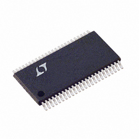
LTC1742IFW Linear Technology, LTC1742IFW Datasheet

LTC1742IFW
Specifications of LTC1742IFW
Related parts for LTC1742IFW
LTC1742IFW Summary of contents
Page 1
... LTC1744 (14-Bit), LTC1743 (12-Bit) 65Msps: LTC1742 (14-Bit), LTC1741 (12-Bit) 80Msps: LTC1748 (14-Bit), LTC1747 (12-Bit) 48-Pin TSSOP Package U APPLICATIO S Telecommunications Receivers Cellular Base Stations Spectrum Analysis Imaging Systems , LTC and LT are registered trademarks of Linear Technology Corporation. W BLOCK DIAGRA + DIFFERENTIAL ANALOG INPUT – A ...
Page 2
... External Reference (SENSE = 1.6V) Internal Reference SENSE = 1.6V CONDITIONS 4.75V V 5.25V DD + – 0 < < Sample Mode ENC < ENC Hold Mode ENC > ENC – + 1.5V < < INFORMATION ORDER PART TOP VIEW NUMBER OGND LTC1742CFW 46 D13 45 D12 LTC1742IFW 44 D11 D10 OGND 37 GND 36 GND OGND ...
Page 3
ACCURACY SYMBOL PARAMETER SNR Signal-to-Noise Ratio SFDR Spurious Free Dynamic Range S/( Signal-to-(Noise + Distortion) Ratio THD Total Harmonic Distortion IMD Intermodulation Distortion Sample-and-Hold Bandwidth TER AL REFERE CE ...
Page 4
LTC1742 U U DIGITAL I PUTS A D DIGITAL OUTPUTS operating temperature range, otherwise specifications are at T SYMBOL PARAMETER V High Level Input Voltage IH V Low Level Input Voltage IL I Digital Input Current IN C Digital Input ...
Page 5
ELECTRICAL CHARACTERISTICS Note 1: Absolute Maximum Ratings are those values beyond which the life of a device may be impaired. Note 2: All voltage values are with respect to ground with GND (unless otherwise noted). Note 3: When these pin ...
Page 6
LTC1742 W U TYPICAL PERFOR A CE CHARACTERISTICS 8192 Point FFT, Input Frequency = 30MHz, –10dB, 3.2V Range –10 –20 –30 –40 –50 –60 –70 –80 –90 –100 –110 –120 ...
Page 7
W U TYPICAL PERFOR A CE CHARACTERISTICS 8192 Point FFT, Input Frequency = 70MHz, –10dB, 3.2V Range –10 –20 –30 –40 –50 –60 –70 –80 –90 –100 –110 –120 ...
Page 8
LTC1742 W U TYPICAL PERFOR A CE CHARACTERISTICS SFDR vs Input Frequency and Amplitude, 3.2V Range, 2nd and 3rd Harmonic 100 –20dB 95 –10dB 90 –6dB 85 80 –1dB ...
Page 9
CTIO S SENSE (Pin 1): Reference Sense Pin. Ground selects 1V. V selects 1.6V. Greater than 1V and less than 1.6V DD applied to the SENSE pin selects an input range of V 1.6V is ...
Page 10
LTC1742 DIAGRA • N ANALOG INPUT t 3 ENC t 7 DATA t 6 CLKOUT DATA U U APPLICATIO S I FOR ATIO DYNAMIC PERFORMANCE Signal-to-Noise Plus Distortion Ratio ...
Page 11
U U APPLICATIO S I FOR ATIO Spurious Free Dynamic Range (SFDR) Spurious free dynamic range is the peak harmonic or spurious noise that is the largest spectral component excluding the input signal and DC. This value is expressed in ...
Page 12
LTC1742 U U APPLICATIO S I FOR ATIO In operation, the ADC quantizes the input to the stage and the quantized value is subtracted from the input by the DAC to produce a residue. The residue is amplified and output ...
Page 13
U U APPLICATIO S I FOR ATIO Input Drive Impedance As with all high performance, high speed ADCs the dy- namic performance of the LTC1742 can be influenced by the input drive circuitry, particularly the second and third harmonics. Source ...
Page 14
LTC1742 U U APPLICATIO S I FOR ATIO mode voltage of any external input circuitry; additionally, the reference is used with a difference amplifier to gener- ate the differential reference levels needed by the internal ADC circuitry. An external bypass ...
Page 15
U U APPLICATIO S I FOR ATIO ANALOG INPUT 0.1 F CLOCK INPUT 50 ENC THRESHOLD 2V ENC 0.1 F Figure 8a. Single-Ended ENC Drive, Not Recommended for Low Jitter Any noise present on the encode signal ...
Page 16
LTC1742 U U APPLICATIO S I FOR ATIO At sample rates slower than 65Msps the duty cycle can vary from 50% as long as each half cycle is at least 7.3ns. The lower limit of the LTC1742 sample rate is ...
Page 17
U U APPLICATIO S I FOR ATIO OV can be powered with any voltage up to 5V. The logic DD outputs will swing between OGND and OV Output Enable The outputs may be disabled with the output enable pin, OE. ...
Page 18
LTC1742 U U APPLICATIO S I FOR ATIO 1742f ...
Page 19
... APPLICATIO S I FOR ATIO Silkscreen Top Layer 2 GND Plane Information furnished by Linear Technology Corporation is believed to be accurate and reliable. However, no responsibility is assumed for its use. Linear Technology Corporation makes no represen- tation that the interconnection of its circuits as described herein will not infringe on existing patent rights ...
Page 20
... Pin Compatible with the LTC1742 Pin Compatible with the LTC1742 Rail-to-Rail Input and Output www.linear.com 7.9 – 8.3 (.311 – .327) 1.20 (.0473) MAX -T- .10 C FW48 TSSOP 0502 0.05 – 0.15 (.002 – .006) 1742f LT/TP 0603 1K • PRINTED IN THE USA LINEAR TECHNOLOGY CORPORATION 2003 ...


