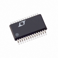
LTC1605ACG#TRPBF Linear Technology, LTC1605ACG#TRPBF Datasheet - Page 9

LTC1605ACG#TRPBF
Manufacturer Part Number
LTC1605ACG#TRPBF
Description
IC A/D CONV 16BIT SAMPLNG 28SSOP
Manufacturer
Linear Technology
Datasheet
1.LTC1605INPBF.pdf
(16 pages)
Specifications of LTC1605ACG#TRPBF
Number Of Bits
16
Sampling Rate (per Second)
100k
Data Interface
Parallel
Number Of Converters
1
Power Dissipation (max)
80mW
Voltage Supply Source
Analog and Digital
Operating Temperature
0°C ~ 70°C
Mounting Type
Surface Mount
Package / Case
28-SSOP (0.200", 5.30mm Width)
Lead Free Status / RoHS Status
Lead free / RoHS Compliant
Available stocks
Company
Part Number
Manufacturer
Quantity
Price
APPLICATIONS
For minimum code transition noise the REF pin and the
CAP pin should each be decoupled with a capacitor to
filter wideband noise from the reference and the buffer
(2.2µF tantalum).
Offset and Gain Adjustments
The LTC1605 offset and full-scale errors have been trimmed
at the factory with the external resistors shown in Figure 4.
This allows for external adjustment of offset and full scale
in applications where absolute accuracy is important. See
Figure 5 for the offset and gain trim circuit. First adjust the
offset to zero by adjusting resistor R3. Apply an input
voltage of –152.6mV (– 0.5LSB) and adjust R3 so the code
is changing between 1111 1111 1111 1111 and 0000 0000
0000 0000. The gain error is trimmed by adjusting resistor
R4. An input voltage of 9.999542V (+FS – 1.5LSB) is
Internal Voltage Reference
The LTC1605 has an on-chip, temperature compensated,
curvature corrected, bandgap reference, which is factory
trimmed to 2.50V. The full-scale range of the ADC is equal
to (±4 • V
reference is connected to the input of a unity-gain buffer
through a 4k resistor (see Figure 3). The input to the buffer
or the output of the reference is available at REF (Pin 3).
The internal reference can be overdriven with an external
reference if more accuracy is needed. The buffer output
drives the internal DAC and is available at CAP (Pin 4). The
CAP pin can be used to drive a steady DC load of less than
2mA. Driving an AC load is not recommended because it
can cause the performance of the converter to degrade.
(2.5V)
(2.5V)
2.2µF
2.2µF
Figure 3. Internal or External Reference Source
CAP
REF
REF
) or nominally ±10V. The output of the
3
4
S
S
U
+
–
INFORMATION
U
4k
W
V
ANA
1605 • F03
REFERENCE
CAPACITOR
BANDGAP
INTERNAL
DAC
U
applied to V
changing between 0111 1111 1111 1110 and 0111 1111
1111 1111. Figure 6 shows the bipolar transfer character-
istic of the LTC1605.
DC Performance
One way of measuring the transition noise associated with
a high resolution ADC is to use a technique where a DC
±10V INPUT
±10V INPUT
Figure 6. LTC1605 Bipolar Transfer Characteristics
011...111
011...110
000...001
000...000
111...111
111...110
100...001
100...000
Figure 5. ±10V Input with Offset and Gain Trim
200Ω
IN
1%
33.2k
Figure 4. ±10V Input Without Trim
200Ω
1%
and R4 is adjusted until the output code is
1%
–FS/2
+
5V
33.2k
1%
R3
50k
2.2µF
50k
INPUT VOLTAGE (V)
R4
BIPOLAR
+
–1
LSB
+
ZERO
+
2.2µF
0V
576k
2.2µF
2.2µF
1
2
3
4
5
LSB
FS = 20V
1LSB = FS/65536
1
V
AGND1
REF
CAP
AGND2
IN
1
2
3
4
5
LTC1605
V
AGND1
REF
CAP
AGND2
FS/2 – 1LSB
IN
1605 • F06
LTC1605
LTC1605
1605 • F04
1605 • F05
1605fc
9


