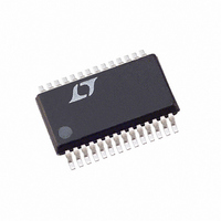
LTC1605-2CG#TR Linear Technology, LTC1605-2CG#TR Datasheet - Page 10

LTC1605-2CG#TR
Manufacturer Part Number
LTC1605-2CG#TR
Description
IC ADC 16BIT 5V SAMPLING 28SSOP
Manufacturer
Linear Technology
Datasheet
1.LTC1605-1CGPBF.pdf
(20 pages)
Specifications of LTC1605-2CG#TR
Number Of Bits
16
Sampling Rate (per Second)
100k
Data Interface
Parallel
Number Of Converters
1
Power Dissipation (max)
80mW
Voltage Supply Source
Analog and Digital
Operating Temperature
0°C ~ 70°C
Mounting Type
Surface Mount
Package / Case
28-SSOP (0.200", 5.30mm Width)
Lead Free Status / RoHS Status
Contains lead / RoHS non-compliant
Available stocks
Company
Part Number
Manufacturer
Quantity
Price
LTC1605-1/LTC1605-2
APPLICATIONS
DIGITAL INTERFACE
Internal Clock
The ADC has an internal clock that is trimmed to achieve
a typical conversion time of 7 s. No external adjustments
are required and, with the typical acquisition time of 1 s,
throughput performance of 100ksps is assured.
Timing and Control
Conversion start and data read are controlled by two
digital inputs: CS and R/C. To start a conversion and put
the sample-and-hold into the hold mode, bring CS and
R/C low for no less than 40ns. Once initiated, it cannot be
restarted until the conversion is complete. Converter
status is indicated by the BUSY output and this is low
while the conversion is in progress.
There are two modes of operation. The first mode is
shown in Figure 8. The digital input R/C is used to control
the start of conversion. CS is tied low. When R/C goes
low, the sample-and-hold goes into the hold mode and a
conversion is started. BUSY goes low and stays low
during the conversion and will go back high after the
conversion has been completed and the internal output
shift registers have been updated. R/C should remain low
for no less than 40ns. During the time R/C is low, the
10
DATA MODE
MODE
BUSY
R/C
DATA VALID
PREVIOUS
ACQUIRE
U
t
6
Figure 8. Conversion Timing with Outputs Enabled After Conversion (CS Tied Low)
INFORMATION
U
t
t
3
7
t
1
HI-Z
W
t
9
CONVERT
t
DATA VALID
CONV
PREVIOUS
U
t
2
t
4
t
11
NOT VALID
digital outputs are in a Hi-Z state. R/C should be brought
back high within 3 s after the start of the conversion to
ensure that no errors occur in the digitized result. The
second mode, shown in Figure 9, uses the CS signal to
control the start of a conversion and the reading of the
digital output. In this mode, the R/C input signal should
be brought low no less than 10ns before the falling edge
of CS. The minimum pulse width for CS is 40ns. When CS
falls, BUSY goes low and will stay low until the end of the
conversion. BUSY will go high after the conversion has
been completed. The new data is valid when CS is
brought back low again to initiate a read. Again, it is
recommended that both R/C and CS return high within
3 s after the start of the conversion.
Output Data
The output data can be read as a 16-bit word or it can be
read as two 8-bit bytes. The format of the output data is
straight binary for the LTC1605-1 and two’s complement
for the LTC1605-2. The digital input pin BYTE is used to
control the two byte read. With the BYTE pin low, the first
eight MSBs are output on the D15 to D8 pins and the eight
LSBs are output on the D7 to D0 pins. When the BYTE pin
is taken high, the eight LSBs replace the eight MSBs
(Figure 10).
ACQUIRE
t
5
t
8
t
ACQ
VALID
DATA
CONVERT
HI-Z
1605-1/2 F08
VALID
DATA


