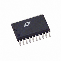
LTC1609ISW Linear Technology, LTC1609ISW Datasheet - Page 12

LTC1609ISW
Manufacturer Part Number
LTC1609ISW
Description
IC A/DCONV 16BIT SRL SAMP 20SOIC
Manufacturer
Linear Technology
Datasheet
1.LTC1609CSW.pdf
(24 pages)
Specifications of LTC1609ISW
Number Of Bits
16
Sampling Rate (per Second)
200k
Data Interface
Serial
Number Of Converters
1
Power Dissipation (max)
100mW
Voltage Supply Source
Analog and Digital
Operating Temperature
-40°C ~ 85°C
Mounting Type
Surface Mount
Package / Case
20-SOIC (0.300", 7.50mm Width)
Lead Free Status / RoHS Status
Contains lead / RoHS non-compliant
Available stocks
Company
Part Number
Manufacturer
Quantity
Price
Company:
Part Number:
LTC1609ISW
Manufacturer:
SONY
Quantity:
6 232
Part Number:
LTC1609ISW
Manufacturer:
LT/凌特
Quantity:
20 000
Company:
Part Number:
LTC1609ISW#PBF
Manufacturer:
Linear Technology
Quantity:
135
APPLICATIO S I FOR ATIO
LTC1609
Table 1c. LTC1609 Output Codes for Ideal Input Voltages
DESCRIPTION
Full-Scale Range
Least Significant Bit
+Full Scale (FS – 1LSB) 9.999695V 4.999847V 3.339898V
Midscale
1LSB Below Midscale
– Full Scale
The ideal FS value for the 3.3V range is 3.340000V – 1LSB
and – 3.340000V, respectively. The external 33.2k resistor
that is connected between the CAP pin and the R2
slightly attenuates the input signal applied to R2
out the 33.2k resistor the FS value would be 3.333333V
– 1LSB and – 3.333333V (zero volt offset), respectively.
DC Performance
One way of measuring the transition noise associated with
a high resolution ADC is to use a technique where a DC
signal is applied to the input of the ADC and the resulting
output codes are collected over a large number of conver-
sions. For example in Figure 5 the distribution of output
code is shown for a DC input that has been digitized 4096
times. The distribution is Gaussian and the RMS code
transition is about 0.9LSB.
12
Figure 4a. LTC1609 Bipolar Transfer Characteristics
011...111
011...110
000...001
000...000
111...111
111...110
100...001
100...000
–FSR/2
U
– 305 V
305 V
–10V
INPUT VOLTAGE (V)
10V
0V
BIPOLAR
U
LSB
–1
ZERO
0V
FSR = +FS – –FS
1LSB = FSR/65536
–153 V
153 V
LSB
1
– 5V
0V
5V
W
FSR/2 – 1LSB
– 3.340000V
1609 F04a
–102 V
102 V
3.34
0V
ANALOG INPUT
U
IN
. With-
9.999847V 4.999924V 3.999939V 0111 1111 1111 1111
4.999847V 2.499924V 1.999939V 1111 1111 1111 1111
IN
0V to 10V
153 V
pin,
5V
0V
0V to 5V
76 V
2.5V
0V
Figure 4b. LTC1609 Unipolar Transfer Characteristics
111...111
111...110
100...001
100...000
011...111
011...110
000...001
000...000
2000
1500
1000
500
0V to 4V
Figure 5. Histogram for 4096 Conversions
61 V
0
2V
0V
–3
0V
–2
TWO’S COMPLEMENT
0000 0000 0000 0000
1000 0000 0000 0000
INPUT VOLTAGE (V)
(SB/BTC LOW)
–1
CODE
0
1LSB = FS/65536
1
2
FS – 1LSB
1111 1111 1111 1111
1000 0000 0000 0000
0111 1111 1111 1111
0000 0000 0000 0000
1609 F04b
1609 F05
STRAIGHT BINARY
3
(SB/BTC HIGH)
1609fa


