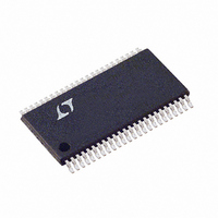
LTC1851CFW Linear Technology, LTC1851CFW Datasheet - Page 22

LTC1851CFW
Manufacturer Part Number
LTC1851CFW
Description
IC ADC 12BIT 1.25MSPS 48-TSSOP
Manufacturer
Linear Technology
Datasheet
1.LTC1851CFWPBF.pdf
(28 pages)
Specifications of LTC1851CFW
Number Of Bits
12
Sampling Rate (per Second)
1.25M
Data Interface
Parallel
Number Of Converters
1
Power Dissipation (max)
50mW
Voltage Supply Source
Single Supply
Operating Temperature
0°C ~ 70°C
Mounting Type
Surface Mount
Package / Case
48-TFSOP (0.240", 6.10mm Width)
Lead Free Status / RoHS Status
Contains lead / RoHS non-compliant
Available stocks
Company
Part Number
Manufacturer
Quantity
Price
Company:
Part Number:
LTC1851CFW
Manufacturer:
ABOV
Quantity:
270
Part Number:
LTC1851CFW
Manufacturer:
LT/凌特
Quantity:
20 000
Company:
Part Number:
LTC1851CFW#PBF
Manufacturer:
AD
Quantity:
21
APPLICATIO S I FOR ATIO
LTC1850/LTC1851
In slow memory mode, the processor applies a logic low
to RD ( = CONVST), starting the conversion. BUSY goes
low, forcing the processor into a Wait state. The previous
conversion result appears on the data outputs. When the
conversion is complete, the new conversion results ap-
pear on the data outputs; BUSY goes high releasing the
processor, and the processor takes RD ( = CONVST) back
high and reads the new conversion data.
In ROM mode, the processor takes RD ( = CONVST) low,
starting a conversion and reading the previous conversion
result. After the conversion is complete, the processor can
read the new result and initiate another conversion.
MODES OF OPERATION
Direct Address Mode
The simplest mode of operation is the Direct Address
mode. This mode is selected when both the M1 and M0
pins are low. In this mode, the address input pins directly
control the MUX and the configuration input pins directly
control the input span. The address and configuration
input pins are enabled when WR is low. WR can be tied low
if the pins will be constantly driven or the rising edge of WR
can be used to latch and hold the inputs for as long as WR
is held high.
Scan Mode
Scan mode is selected when M1 is low and M0 is high. This
mode allows the converter to scan through all of the input
channels sequentially and repeatedly without the user
having to provide an address. The address input pins (A2
to A0) are ignored but the DIFF, PGA and UNI/BIP pins are
still enabled when WR is low. As in the direct address
mode, WR can be held low or the rising edge of WR can be
used to latch and hold the information on these pins for as
long as WR is held high. The DIFF pin selects the scan
pattern. If DIFF is held low, the scan pattern will consist of
all eight channels in succession, single-ended relative to
COM (CH0-COM, CH1-COM, CH2-COM, CH3-COM,
22
U
U
W
U
CH4-COM, CH5-COM, CH6-COM, CH7-COM, repeat). At
the maximum conversion rate the throughput rate for each
channel would be 1.25Msps/8 or 156.25ksps. If DIFF is
held high, the scan pattern will consist of four differential
pairs (CH0-CH1, CH2-CH3, CH4-CH5, CH6-CH7, repeat).
At the maximum conversion rate, the throughput rate for
each pair would be 1.25Msps/4 or 312.5ksps. It is pos-
sible to drive the DIFF input pin while the part is in Scan
mode to achieve combinations of single-ended and differ-
ential inputs. For instance, if the A0
DIFF input pin, the scan pattern will consist of four single-
ended inputs and two differential pairs (CH0-COM single-
ended, CH1-COM single-ended, CH2-CH3 differential,
CH4-COM single-ended, CH5-COM single-ended, CH6-
CH7 differential, repeat).
The scan counter is reset to zero whenever the M0 pin
changes state so that the first conversion after M0 rises
will be MUX Address 000 (CH0-COM single-ended or CH0-
CH1 differential depending on the state of the DIFF pin). A
conversion is initiated by the falling edge of CONVST. After
each conversion, the address counter is advanced (by one
if DIFF is low, by two if DIFF is high) and the MUX address
for the present conversion is available on the address
output pins (DIFF
conversion result.
Program/Readback Mode
The LTC1850/LTC1851 include a sequencer that can be
programmed to run a sequence of up to 16 locations
containing a MUX address and input configuration. The
MUX address and input configuration for each location are
programmed using the DIFF, A2 to A0, UNI/BIP and PGA
pins and are stored in memory along with an end-of-
sequence (EOS) bit that is generated automatically. The
six input address and configuration bits plus the EOS bit
can be read back by accessing the 7-bit readback status
word (S6-S0) through the data output pins. The sequencer
memory is a 16 7 block of memory represented by the
block diagram in Figure 10.
OUT
, A2
OUT
to A0
OUT
OUT
) along with the
pin is tied to the
18501f


