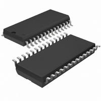
LTC1410ISW Linear Technology, LTC1410ISW Datasheet - Page 10

LTC1410ISW
Manufacturer Part Number
LTC1410ISW
Description
IC A/D CONV 12BIT SAMPLNG 28SOIC
Manufacturer
Linear Technology
Datasheet
1.LTC1410CSWPBF.pdf
(16 pages)
Specifications of LTC1410ISW
Number Of Bits
12
Sampling Rate (per Second)
1.25M
Data Interface
Parallel
Number Of Converters
1
Power Dissipation (max)
230mW
Voltage Supply Source
Dual ±
Operating Temperature
-40°C ~ 85°C
Mounting Type
Surface Mount
Package / Case
28-SOIC (0.300", 7.50mm Width)
Lead Free Status / RoHS Status
Contains lead / RoHS non-compliant
Other names
LTC1410IS
Available stocks
Company
Part Number
Manufacturer
Quantity
Price
Part Number:
LTC1410ISW
Manufacturer:
LINEAR/凌特
Quantity:
20 000
LTC1410
capacitors at the end of conversion. During conversion
the analog inputs draw only a small leakage current. If the
source impedance of the driving circuit is low then the
LTC1410 inputs can be driven directly. As source imped-
ance increases so will acquisition time (see Figure 6). For
minimum acquisition time with high source impedance,
a buffer amplifier should be used. The only requirement
is that the amplifier driving the analog input(s) must
settle after the small current spike before the next conver-
sion starts (settling time must be 100ns for full through-
put rate).
Choosing an input amplifier is easy if a few requirements
are taken into consideration. First, choose an amplifier
that has a low output impedance (< 100 ) at the closed-
loop bandwidth frequency. For example, if an amplifier is
used in a gain of +1 and has a closed-loop bandwidth of
50MHz, then the output impedance at 50MHz must be
less than 100 . The second requirement is that the
closed-loop bandwidth must be greater than 20MHz to
ensure adequate small-signal settling for full throughput
rate. If slower op amps are used, more settling time can
be provided by increasing the time between conversions.
Suitable devices capable of driving the ADC’s inputs
include the LT
LT1227 op amps.
The noise and the distortion of the input amplifier must
also be considered since they will add to the LTC1410
noise and distortion. The small-signal bandwidth of the
10
APPLICATIONS
Figure 6. Acquisition Time vs Source Resistance
0.01
0.1
10
1
10
®
1360, LT1220, LT1223, LT1224 and
U
100
SOURCE RESISTANCE ( )
INFORMATION
U
1k
W
10k
1410 F06
100k
U
sample-and-hold circuit is 20MHz. Any noise that is present
at the analog inputs will be summed over this entire
bandwidth. Noisy input circuitry should be filtered prior to
the analog inputs to minimize noise. A simple 1-pole RC
filter is usually sufficient. For example, Figure 7 shows a
1000pF capacitor from + A
resistor will limit the input bandwidth to 1.6MHz. Simple
RC filters work well for AC applications, but they will limit
the transient response. For full speed operation, amplifiers
with fast settling and low noise should be chosen.
Internal Reference
The LTC1410 has an on-chip, temperature compensated,
curvature corrected, bandgap reference which is factory
trimmed to 2.500V. It is connected internally to a reference
amplifier and is available at V
2k resistor is in series with the output so that it can be
2.500V
ANALOG
INPUT
ANALOG
INPUT
10 F
Figure 8a. LTC1410 Reference Circuit
4.06V
10 F
100
0.1 F
Figure 7. RC Input Filter
1
2
3
4
5
REFCOMP
AGND
+A
–A
V
1000pF
REF
0.1 F
IN
IN
IN
40k
R2
to ground and a 100 source
REF
1
2
3
4
5
64k
R3
+A
–A
V
REFCOMP
AGND
(Pin 3). See Figure 8a. A
REF
IN
IN
+
–
LTC1410
LTC1410
R1
2k
REFERENCE
BANDGAP
1410 F07
1410 F08a


