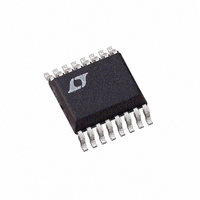
LTC2440CGN#PBF Linear Technology, LTC2440CGN#PBF Datasheet - Page 14

LTC2440CGN#PBF
Manufacturer Part Number
LTC2440CGN#PBF
Description
IC ADC DIFFER 24-BIT HS 16-SSOP
Manufacturer
Linear Technology
Datasheet
1.LTC2440CGN.pdf
(28 pages)
Specifications of LTC2440CGN#PBF
Number Of Bits
24
Sampling Rate (per Second)
3.5k
Data Interface
MICROWIRE™, Serial, SPI™
Number Of Converters
2
Power Dissipation (max)
40mW
Voltage Supply Source
Single Supply
Operating Temperature
0°C ~ 70°C
Mounting Type
Surface Mount
Package / Case
16-SSOP (0.150", 3.90mm Width)
Number Of Elements
1
Resolution
24Bit
Architecture
Delta-Sigma
Sample Rate
4KSPS
Input Polarity
Bipolar
Input Type
Voltage
Rated Input Volt
±2.75V
Differential Input
Yes
Power Supply Requirement
Single
Single Supply Voltage (typ)
5V
Single Supply Voltage (min)
4.5V
Single Supply Voltage (max)
5.5V
Dual Supply Voltage (typ)
Not RequiredV
Dual Supply Voltage (min)
Not RequiredV
Dual Supply Voltage (max)
Not RequiredV
Differential Linearity Error
±1LSB(Typ)
Integral Nonlinearity Error
15ppm of Vref
Operating Temp Range
0C to 70C
Operating Temperature Classification
Commercial
Mounting
Surface Mount
Pin Count
16
Package Type
SSOP N
Input Signal Type
Differential
Lead Free Status / RoHS Status
Lead free / RoHS Compliant
Available stocks
Company
Part Number
Manufacturer
Quantity
Price
LTC2440
APPLICATIONS INFORMATION
Table 4. LTC2440 Interface Timing Modes
Confi guration
External SCK, Single Cycle Conversion
External SCK, 2-Wire I/O
Internal SCK, Single Cycle Conversion
Internal SCK, 2-Wire I/O, Continuous Conversion
14
Table 3. SDI Speed/Resolution Programming
**Address allows tying SDI HIGH *Additional address to allow tying SDI LOW
OSR4
BUSY
X
X
X
X
X
X
X
X
X
X
SDO
0
SCK
SDI
CS
*OSR4 BIT MUST BE AT FIRST SCK RISING EDGE DURING SERIAL DATA OUT CYCLE
OSR3
Hi-Z
0
0
0
0
0
0
0
0
1
1
1
OSR2
0
0
0
0
1
1
1
1
0
0
1
BIT 31
OSR4*
EOC
OSR1
0
1
0
1
0
0
1
1
0
0
1
BIT 30
OSR3
“0”
Figure 4. SDI Speed/Resolution Programming
OSR0
1
0
0
1
0
1
0
1
0
1
1
OSR2
BIT 29
SIG
External
External
Internal
Internal
Source
SCK
9MHz CLOCK
BIT 28
OSR1
MSB
INTERNAL
13.75Hz
6.875Hz
3.52kHz
1.76kHz
27.5Hz
880Hz
880Hz
440Hz
220Hz
110Hz
55Hz
CONVERSION RATE
BIT 27
OSR0
CS and SCK
Conversion
Continuous
BIT 26
Control
Cycle
10.24MHz CLOCK
SCK
CS
EXTERNAL
15.625Hz
7.8125Hz
31.25Hz
↑
62.5Hz
500Hz
250Hz
125Hz
4kHz
2kHz
1kHz
1kHz
BIT 25
BIT 1
NOISE
750nV
510nV
375nV
250nV
200nV
3.5μV
1.4μV
CS and SCK
23μV
RMS
2μV
2μV
1μV
Control
Internal
Output
Data
SCK
CS
BIT 0
LSB
↑
ENOB
21.3
21.3
21.8
22.4
22.9
23.4
24.4
24.6
17
20
24
2440 F04
Hi-Z
32768**
16384
256*
1024
2048
4096
8192
OSR
128
256
512
64
Waveforms
Figures 5, 6
Figures 8, 9
Connection
Figure 10
Figure 7
and
2440fd


