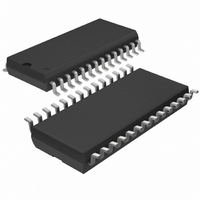
LTC1410CSW Linear Technology, LTC1410CSW Datasheet - Page 11

LTC1410CSW
Manufacturer Part Number
LTC1410CSW
Description
IC A/D CONV 12BIT SAMPLNG 28SOIC
Manufacturer
Linear Technology
Datasheet
1.LTC1410CSWPBF.pdf
(16 pages)
Specifications of LTC1410CSW
Number Of Bits
12
Sampling Rate (per Second)
1.25M
Data Interface
Parallel
Number Of Converters
1
Power Dissipation (max)
230mW
Voltage Supply Source
Dual ±
Operating Temperature
0°C ~ 70°C
Mounting Type
Surface Mount
Package / Case
28-SOIC (0.300", 7.50mm Width)
Lead Free Status / RoHS Status
Contains lead / RoHS non-compliant
Other names
LTC1410CS
Available stocks
Company
Part Number
Manufacturer
Quantity
Price
Part Number:
LTC1410CSW
Manufacturer:
LINEAR/凌特
Quantity:
20 000
APPLICATIONS
Full-Scale and Offset Adjustment
Figure 9 shows the ideal input/output characteristics for
the LTC1410. The code transitions occur midway between
successive integer LSB values (i.e., – FS + 0.5LSB,
– FS + 1.5LSB, – FS + 2.5LSB, . . . FS – 1.5LSB,
FS – 0.5LSB).The output is two’s complement binary
with 1LSB = [(+FS) – (– FS)]/4096 = 5V/4096 = 1.22mV.
In applications where absolute accuracy is important,
offset and full-scale errors can be adjusted to zero. Offset
error must be adjusted before full-scale error. Figure 10
shows the extra components required for full-scale error
adjustment. Zero offset is achieved by adjusting the offset
applied to the – A
– 0.61mV (i.e., – 0.5LSB) at +A
the – A
0000 0000 and 1111 1111 1111. For full-scale adjust-
ment, an input voltage of 2.49817V (FS – 1.5LSBs) is
easily overdriven in applications where an external refer-
ence is required. The reference amplifier provides buffer-
ing between the internal reference and the capacitive DAC.
The reference amplifier compensation pin REFCOMP
(Pin 4), must be bypassed with a capacitor to ground. The
reference amplifier is stable with capacitors of 1 F or
greater. For the best noise performance, a 10 F tantalum
in parallel with 0.1 F ceramic is recommended.
The V
(Figure 8b), a DAC or other means to provide input span
adjustment. The V
to 2.75V for specified linearity.
Figure 8b. Using the LT1019-2.5 as an External Reference
REF
LT1019A-2.5
IN
input until the output code flickers between 0000
V
5V
pin can be driven with an external reference
IN
V
OUT
REF
IN
U
10 F
should be kept in the range of 2.25V
input. For zero offset error apply
ANALOG
INPUT
INFORMATION
U
0.1 F
IN
1
2
3
4
5
and adjust the offset at
+A
–A
V
REFCOMP
AGND
W
REF
IN
IN
LTC1410
U
1410 F08b
applied to A
flickers between 0111 1111 1110 and 0111 1111 1111.
BOARD LAYOUT AND BYPASSING
Wire wrap boards are not recommended for high resolu-
tion or high speed A/D converters. To obtain the best
performance from the LTC1410, a printed circuit board
with ground plane is required. Layout for the printed
circuit board should ensure that digital and analog signal
lines are separated as much as possible. Particular care
should be taken not to run any digital track alongside an
analog signal track or underneath the ADC. The analog
input should be screened by AGND.
50k
R1
– 5V
Figure 10. Offset and Full-Scale Adjust Circuit
10 F
011...111
011...110
000...001
000...000
111...111
111...110
100...001
100...000
R5
47k
Figure 9. LTC1410 Transfer Characteristics
IN
50k
R2
and R2 is adjusted until the output code
47k
R3
–FS
R6
24k
INPUT VOLTAGE, (+A
0.1 F
100
ANALOG
R4
INPUT
BIPOLAR
LSB
–1
ZERO
0V
IN
LSB
) – (–A
1
4
2
3
5
1
FS = 2.5V
1LSB =
+A
–A
V
REFCOMP
AGND
REF
IN
IN
IN
) (V)
FS – LSB
LTC1410
4096
LTC1410
2FS
1410 F09
11
1410 F10


