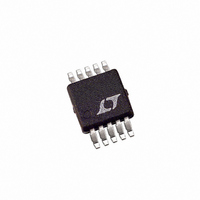
LTC1403AIMSE Linear Technology, LTC1403AIMSE Datasheet - Page 14

LTC1403AIMSE
Manufacturer Part Number
LTC1403AIMSE
Description
IC ADC 14BIT 2.8MSPS DIFF 10MSOP
Manufacturer
Linear Technology
Datasheet
1.LTC1403CMSEPBF.pdf
(20 pages)
Specifications of LTC1403AIMSE
Number Of Bits
14
Sampling Rate (per Second)
2.8M
Data Interface
Serial, SPI™
Number Of Converters
1
Power Dissipation (max)
12mW
Voltage Supply Source
Single Supply
Operating Temperature
-40°C ~ 125°C
Mounting Type
Surface Mount
Package / Case
10-TFSOP, 10-MSOP (0.118", 3.00mm Width) Exposed Pad
Lead Free Status / RoHS Status
Contains lead / RoHS non-compliant
Available stocks
Company
Part Number
Manufacturer
Quantity
Price
Company:
Part Number:
LTC1403AIMSE
Manufacturer:
LT
Quantity:
10 000
Part Number:
LTC1403AIMSE
Manufacturer:
LT
Quantity:
20 000
Part Number:
LTC1403AIMSE#PBF
Manufacturer:
LT/凌特
Quantity:
20 000
Company:
Part Number:
LTC1403AIMSE-1
Manufacturer:
LT
Quantity:
10 000
Company:
Part Number:
LTC1403AIMSE-1#PBF
Manufacturer:
LT
Quantity:
1 000
Part Number:
LTC1403AIMSE-1#PBF
Manufacturer:
LINEAR/凌特
Quantity:
20 000
Company:
Part Number:
LTC1403AIMSE-1#TRPBF
Manufacturer:
LT
Quantity:
1 000
APPLICATIONS INFORMATION
LTC1403/LTC1403A
fi rst and then buffer this signal with the appropriate number
of inverters to drive the serial clock input of the processor
serial port. Use the falling edge of the clock to latch data
from the Serial Data Output (SDO) into your processor
serial port. The 14-bit Serial Data will be received right
justifi ed, in a 16-bit word with 16 or more clocks per frame
sync. It is good practice to drive the LTC1403/LTC1403A
SCK input fi rst to avoid digital noise interference during
the internal bit comparison decision by the internal high
speed comparator. Unlike the CONV input, the SCK input
is not sensitive to jitter because the input signal is already
sampled and held constant.
Serial Data Output (SDO)
Upon power-up, the SDO output is automatically reset to
the high impedance state. The SDO output remains in high
impedance until a new conversion is started. SDO sends
out 12/14 bits in the output data stream beginning at the
third rising edge of SCK after the rising edge of CONV.
SDO is always in high impedance mode when it is not
sending out data bits. Please note the delay specifi cation
from SCK to a valid SDO. SDO is always guaranteed to
be valid by the next rising edge of SCK. The 16-bit output
data stream is compatible with the 16-bit or 32-bit serial
port of most processors.
14
LTC1403/
LTC1403A
CONV
GND
SDO
SCK
V
DD
7
10
9
8
6
3V
Figure 6. DSP Serial Interface to TMS320C54x
CONV
CLK
0V TO 3V LOGIC SWING
INTERFACELINK
3-WIRE SERIAL
HARDWARE INTERFACE TO TMS320C54X
The LTC1403/LTC1403A is a serial output ADC whose
interface has been designed for high speed buffered
serial ports in fast digital signal processors (DSPs).
Figure 6 shows an example of this interface using a
TMS320C54X.
The buffered serial port in the TMS320C54x has direct
access to a 2kB segment of memory. The ADC’s serial
data can be collected in two alternating 1kB segments,
in real time, at the full 2.8Msps conversion rate of the
LTC1403/LTC1403A. The DSP assembly code sets frame
sync mode at the BFSR pin to accept an external posi-
tive going pulse and the serial clock at the BCLKR pin to
accept an external positive edge clock. Buffers near the
LTC1403/LTC1403A may be added to drive long tracks to
the DSP to prevent corruption of the signal to LTC1403/
LTC1403A. This confi guration is adequate to traverse a
typical system board, but source resistors at the buffer
outputs and termination resistors at the DSP, may be
needed to match the characteristic impedance of very
long transmission lines. If you need to terminate the SDO
transmission line, buffer it fi rst with one or two 74ACTxx
gates. The TTL threshold inputs of the DSP port respond
properly to the 3V swing from the SDO pin.
B13
B12
5V
TMS320C54x
V
BFSR
BCLKR
BDR
CC
1403A F09
1403fb


