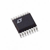
LTC1402IGN Linear Technology, LTC1402IGN Datasheet - Page 14

LTC1402IGN
Manufacturer Part Number
LTC1402IGN
Description
IC ADC 12BIT 2.2MSPS SHDN 16SSOP
Manufacturer
Linear Technology
Datasheet
1.LTC1402CGNPBF.pdf
(24 pages)
Specifications of LTC1402IGN
Number Of Bits
12
Sampling Rate (per Second)
2.2M
Data Interface
MICROWIRE™, Serial, SPI™
Number Of Converters
1
Power Dissipation (max)
150mW
Voltage Supply Source
Analog and Digital, Dual ±
Operating Temperature
-40°C ~ 85°C
Mounting Type
Surface Mount
Package / Case
16-SSOP (0.150", 3.90mm Width)
Lead Free Status / RoHS Status
Contains lead / RoHS non-compliant
Available stocks
Company
Part Number
Manufacturer
Quantity
Price
Company:
Part Number:
LTC1402IGN
Manufacturer:
NEC
Quantity:
6 945
Part Number:
LTC1402IGN#PBF
Manufacturer:
LINEAR/凌特
Quantity:
20 000
Part Number:
LTC1402IGN#TRPBF
Manufacturer:
LINEAR/凌特
Quantity:
20 000
APPLICATIONS
LTC1402
more than 0.25 inch long to the common reference. You
may also choose to tie AGND2 (Pin 6) directly to a solid
analog ground plane and eliminate all the 10 F capacitors
at this pin. The external reference source needs to have
enough output drive current for the 2k load at each ADC.
FULL-SCALE AND OFFSET ADJUSTMENT
Figure 9 shows the ideal input/output characteristics for
the LTC1402 in bipolar mode and unipolar mode. Figure
10a shows the components required for full-scale error
adjustment. Figure 10b includes the components for off-
set and full-scale adjustment.
Adjustment in Bipolar Mode with Pin 8 Held High
The code transitions occur midway between successive
integer LSB values (i.e., – FS + 0.5LSB, – FS + 1.5LSB, – FS
+ 2.5LSB,...FS – 2.5LSB, FS – 1.5LSB). The output at D
is two’s complement binary with 1LSB = FS – (– FS)/4096
= 4.096V/4096 = 1.0mV. In applications where absolute
accuracy is important, offset and full-scale errors can be
adjusted to zero. Offset error must be adjusted before full-
scale error. In Figure 10b, zero offset is achieved by
adjusting the offset applied to the A
offset error, apply – 0.5mV (i.e., – 0.5LSB) to A
adjust the offset at the A
code flickers between 0000 0000 0000 and 1111 1111
1111. For full-scale adjustment in Figures 10a and 10b,
apply an input voltage of 2.0465V (FS – 1.5LSB) to A
and adjust R5 until the output code flickers between 0111
1111 1110 and 0111 1111 1111.
14
011...111
011...110
011...101
100...010
100...001
100...000
Figure 9. LTC1402 Transfer Characteristic
– (FS – 1LSB)
U
INPUT VOLTAGE (V)
IN
INFORMATION
–
U
input using R8 until the output
W
FS – 1LSB
IN
–
1402 F09
input. For zero
111...111
111...110
111...101
000...010
000...001
000...000
U
IN
+
and
OUT
IN
+
Adjustment in Unipolar Mode with Pin 8 Held Low
The code transitions occur midway between successive
integer LSB values (i.e., – FS + 0.5LSB, – FS + 1.5LSB,
D
1.0mV. In applications where absolute accuracy is impor-
tant, offset and full-scale errors can be adjusted to zero.
Offset error must be adjusted before full-scale error. In
Figure 10b, zero offset is achieved by adjusting the offset
applied to the A
– 0.5mV (i.e., – 0.5LSB) to A
A
ANALOG INPUT
FULL-SCALE
– FS + 2.5LSB,...FS – 2.5LSB, FS – 1.5LSB). The output at
ANALOG INPUT
OFFSET
IN
OUT
0V TO 4.096V
0V TO 4.096V
OR 2.048V
OR 2.048V
–
ADJ
input using R8 until the output code flickers between
ADJ
is binary with 1LSB = FS/4096 = 4.096V/4096 =
10k
R8
Figure 10b. Offset and Full-Scale Adjustment
Circuits with 10LSB Range
500
Figure 10a. Full-Scale Adjustment Circuit with
5V
500
R5
10LSB Range
R5
51
51
R1
R3
7.5k
R7
51
51
R4
470k
R1
R3
R4
470k
IN
5V
–
R2
39k
R6
24k
R2
24k
10 F
10 F
input. For zero offset error apply
3
4
5
7
6
6
3
4
5
7
AGND2
A
A
V
GAIN
A
A
V
GAIN
AGND2
IN
IN
REF
IN
IN
REF
+
–
+
–
IN
+
and adjust the offset at the
REFERENCE
S/H
REFERENCE
S/H
64k
64k
64k
64k
AMP
AMP
2.048V
2.048V
REFERENCE
REFERENCE
BANGAP
BANGAP
LTC1402
LTC1402
1402 F010a
1402 F010b


