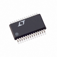
LTC2418CGN Linear Technology, LTC2418CGN Datasheet - Page 19

LTC2418CGN
Manufacturer Part Number
LTC2418CGN
Description
IC ADC 24BIT DIFF INPUT 28SSOP
Manufacturer
Linear Technology
Datasheet
1.LTC2418CGNPBF.pdf
(48 pages)
Specifications of LTC2418CGN
Number Of Bits
24
Sampling Rate (per Second)
7.5
Data Interface
MICROWIRE™, Serial, SPI™
Number Of Converters
1
Power Dissipation (max)
1mW
Voltage Supply Source
Single Supply
Operating Temperature
0°C ~ 70°C
Mounting Type
Surface Mount
Package / Case
28-SSOP (0.150", 3.95mm Width)
Lead Free Status / RoHS Status
Contains lead / RoHS non-compliant
Available stocks
Company
Part Number
Manufacturer
Quantity
Price
Company:
Part Number:
LTC2418CGN#PBF
Manufacturer:
LT
Quantity:
416
APPLICATIO S I FOR ATIO
last input bit A0 of SDI by the time CS pulled HIGH, the
address information is discarded and the previous
address is kept.
Finally, CS can be used to control the free-running modes
of operation, see Serial Interface Timing Modes section.
Grounding CS will force the ADC to continuously convert
at the maximum output rate selected by F
SERIAL INTERFACE TIMING MODES
The LTC2414/LTC2418’s 4-wire interface is SPI and
MICROWIRE compatible. This interface offers several
flexible modes of operation. These include internal/exter-
Table 6. LTC2414/LTC2418 Interface Timing Modes
Configuration
External SCK, Single Cycle Conversion
External SCK, 3-Wire I/O
Internal SCK, Single Cycle Conversion
Internal SCK, 3-Wire I/O, Continuous Conversion
(EXTERNAL)
SDO
SCK
SDI
CS
CONVERSION
Hi-Z
TEST EOC
SLEEP
(OPTIONAL)
TEST EOC
DON’T CARE
U
SLEEP
Hi-Z
U
BIT 31
(1)
EOC
BIT 30
(0)
W
Figure 5. External Serial Clock, Single Cycle Operation
EN
BIT 29
SIG
O
.
0.1V TO V
REFERENCE
ANALOG
INPUTS
VOLTAGE
External
U
External
Internal
Internal
SGL
Source
1µF
BIT 28
2.7V TO 5.5V
MSB
SCK
CC
•
•
•
•
•
•
11
12
21
28
10
9
1
8
ODD/
SIGN
BIT 27
V
REF
REF
CH0
CH7
CH8
CH15
COM
CC
•
•
•
•
•
•
LTC2414/
LTC2418
+
–
GND
SDO
SCK
SDI
A2
BIT 26
CS
F
nal serial clock, 3- or 4-wire I/O, single cycle conversion.
The following sections describe each of these serial inter-
face timing modes in detail. In all these cases, the con-
verter can use the internal oscillator (F
HIGH) or an external oscillator connected to the F
Refer to Table 6 for a summary.
External Serial Clock, Single Cycle Operation
(SPI/MICROWIRE Compatible)
This timing mode uses an external serial clock to shift out
the conversion result and a CS signal to monitor and
control the state of the conversion cycle, see Figure 5.
O
DATA OUTPUT
17
15
20
18
19
16
CS and SCK
Conversion
Continuous
Control
BIT 25
Cycle
CS ↓
A1
SCK
4-WIRE
SPI INTERFACE
V
CC
= 50Hz REJECTION
= EXTERNAL OSCILLATOR
= 60Hz REJECTION
BIT 24
A0
LTC2414/LTC2418
CS and SCK
DON’T CARE
Internal
Control
Output
Data
CS ↓
SCK
BIT 6
LSB
O
PARITY
BIT 0
= LOW or F
Waveforms
Figures 5, 6
Figures 8, 9
Connection
Figure 10
Figure 7
and
CONVERSION
Hi-Z
19
TEST EOC
O
241418fa
pin.
241418 F05
O
=


