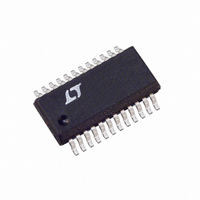
LTC1598LIG#TR Linear Technology, LTC1598LIG#TR Datasheet - Page 22

LTC1598LIG#TR
Manufacturer Part Number
LTC1598LIG#TR
Description
IC ADC 12BIT 3V 8CH SAMPL 24SSOP
Manufacturer
Linear Technology
Datasheet
1.LTC1598LCGPBF.pdf
(24 pages)
Specifications of LTC1598LIG#TR
Number Of Bits
12
Sampling Rate (per Second)
10.5k
Data Interface
MICROWIRE™, QSPI™, Serial, SPI™
Number Of Converters
1
Power Dissipation (max)
480µW
Voltage Supply Source
Single Supply
Operating Temperature
-40°C ~ 85°C
Mounting Type
Surface Mount
Package / Case
24-SSOP (0.200", 5.30mm Width)
Lead Free Status / RoHS Status
Contains lead / RoHS non-compliant
Available stocks
Company
Part Number
Manufacturer
Quantity
Price
LTC1594L/LTC1598L
TYPICAL APPLICATIONS
Using MUXOUT/ADCIN Loop as PGA
This figure shows the LTC1598L’s MUXOUT/ADCIN pins
and an LT1368 being used to create a single channel PGA
with eight noninverting gains. Combined with the LTC1391,
the system can expand to eight channels and eight gains
for each channel. Using the LTC1594L, the PGA is reduced
to four gains. The output of the LT1368 drives the ADCIN
and the resistor ladder. The resistors above the selected
MUX channel form the feedback for the LT1368. The gain
for this amplifier is R
the resistors above the selected MUX channel and R
22
1
2
3
4
5
6
7
8
CH0
CH1
CH2
CH3
CH4
CH5
CH6
CH7
LTC1391
D
GND
CLK
OUT
D
CS
V +
V –
IN
D
16
15
14
13
12
11
10
9
S1
3V
/R
S2
= DAISY CHAIN CONFIGURATION FOR THE LTC1391 AND THE LTC1598L
3(5)
2(6)
+ 1. R
1 F
Using the MUXOUT/ADCIN Pins of the LTC1598L to Form a PGA.
–
+
The LTC1391 MUX Allows Eight Input Channels to be Digitized
1/2 LT1368
U
S1
64R
32R
16R
3V
8R
4R
2R
R
R
8
4
is the summation of
N
1(7)
1 F
20
21
22
23
24
18 MUXOUT
1
2
3
8 COM
CH0
CH1
CH2
CH3
CH4
CH5
CH6
CH7
S2
0.1 F
is
8-CHANNEL
MUX
the summation of the resistors below the selected MUX
channel. If CH0 is selected, the gain is 1 since R
Table 1 shows the gain for each MUX channel. The LT1368
dual rail-to-rail op amp is designed to operate with 0.1 F
load capacitors. These capacitors provide frequency com-
pensation for the amplifiers, help reduce the amplifiers’
output impedance and improve supply rejection at high
frequencies. Because the LT1368’s I
selected channel will not affect the gain given by the
formula above.
17
ADCIN
+
SAMPLING
–
12-BIT
GND
LTC1598L
ADC
16
V
4, 9
REF
V
CC
15, 19
CSMUX
CSADC
D
CLK
OUT
D
NC
NC
IN
12
13
10
6
5, 14
11
7
3V
1 F
B
1594L/98L TA06
is low, the R
P/ C
ON
S1
of the
15948lfb
is 0.


