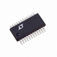
LTC1598IG Linear Technology, LTC1598IG Datasheet - Page 14

LTC1598IG
Manufacturer Part Number
LTC1598IG
Description
IC A/D CONV 12BIT SRL 8CH 24SSOP
Manufacturer
Linear Technology
Datasheet
1.LTC1594CSPBF.pdf
(24 pages)
Specifications of LTC1598IG
Number Of Bits
12
Sampling Rate (per Second)
16.8M
Data Interface
MICROWIRE™, QSPI™, Serial, SPI™
Number Of Converters
1
Power Dissipation (max)
480µW
Voltage Supply Source
Single Supply
Operating Temperature
-40°C ~ 85°C
Mounting Type
Surface Mount
Package / Case
24-SSOP (0.200", 5.30mm Width)
Lead Free Status / RoHS Status
Contains lead / RoHS non-compliant
Available stocks
Company
Part Number
Manufacturer
Quantity
Price
Part Number:
LTC1598IG
Manufacturer:
LT/凌特
Quantity:
20 000
Part Number:
LTC1598IG#PBF
Manufacturer:
LINEAR/凌特
Quantity:
20 000
APPLICATIONS
LTC1594/LTC1598
MUXOUT/ADCIN Loop Economizes
Signal Conditioning
The MUXOUT and ADCIN pins of the LTC1594/LTC1598
form a very flexible external loop that allows Program-
mable Gain Amplifier (PGA) and/or processing analog
input signals prior to conversion. This loop is also a cost
effective way to perform the conditioning, because only
one circuit is needed instead of one for each channel.
In the Typical Applications section, there are a few
examples illustrating how to use the MUXOUT/ADCIN loop
to form a PGA and to antialias filter several analog inputs.
ACHIEVING MICROPOWER PERFORMANCE
With typical operating currents of 320μA and automatic
shutdown between conversions, the LTC1594/LTC1598
achieve extremely low power consumption over a wide
range of sample rates (see Figure 6). The auto shutdown
allows the supply current to drop with reduced sample
rate. Several things must be taken into account to achieve
such a low power consumption.
Shutdown
The LTC1594/LTC1598 are equipped with automatic shut-
down features. They draw power when the CS pin is low.
The bias circuits and comparator of the ADC powers down
and the reference input becomes high impedance at the
end of each conversion leaving the CLK running to clock
out the LSB first data or zeroes (see Figures 1 and 2). When
the CS pin is high, the ADC powers down completely
14
COM = GND
MUXOUT
ADCIN =
CSMUX
CH0 TO
CSADC
D
CLK
CH7
OUT
D
IN
B4
B3 B2
EN
U
D2
B1 B0
D1
D0
INFORMATION
U
t
SMPL
t
ON
t
suCS
Figure 5. Use Separate Chip Selects to Maximize Sample Rate
NULL
BIT
W
B11
B10
DON’T CARE
B9
B8
B7
t
U
CONV
B6
B5
B4
B3 B2
EN
leaving the CLK running to clock the input data word into
MUX. If the CS, D
input logic buffers will draw currents. These currents may
be large compared to the typical supply current. To obtain
the lowest supply current, run the CS, D
rail-to-rail.
D
Capacitive loading on the digital output can increase
power consumption. A 100pF capacitor on the D
can add more than 80mA to the supply current at a
320kHz clock frequency. An extra 80mA or so of current
goes into charging and discharging the load capacitor.
The same goes for digital lines driven at a high frequency
by any logic. The (C)(V)(f) currents must be evaluated
and the troublesome ones minimized.
OUT
D2
B1 B0
Figure 6. Automatic Power Shutdown Between Conversions
Allows Power Consumption to Drop with Sample Rate
D1
Loading
D0
1000
100
t
10
SMPL
1
t
ON
t
0.1
suCS
T
V
V
f
CLK
NULL
A
CC
REF
BIT
= 25°C
= 5V
IN
= 320kHz
= 5V
B11
and CLK are not running rail-to-rail, the
SAMPLE FREQUENCY (kHz)
B10
DON’T CARE
1
B9
B8
B7
t
CONV
B6
10
B5
B4
1594/98 F06
B3 B2
IN
100
EN
and CLK pins
D2
B1 B0
D1
1594/98 F05
OUT
D0
15948fb
pin


