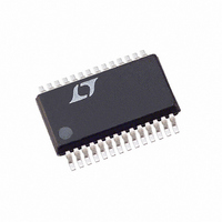
LTC2428IG#PBF Linear Technology, LTC2428IG#PBF Datasheet - Page 19

LTC2428IG#PBF
Manufacturer Part Number
LTC2428IG#PBF
Description
IC ADC 20BIT 8CH MICROPWR 28SSOP
Manufacturer
Linear Technology
Datasheet
1.LTC2424CGPBF.pdf
(36 pages)
Specifications of LTC2428IG#PBF
Number Of Bits
20
Sampling Rate (per Second)
7.5
Data Interface
MICROWIRE™, Serial, SPI™
Number Of Converters
1
Power Dissipation (max)
1mW
Voltage Supply Source
Single Supply
Operating Temperature
-40°C ~ 85°C
Mounting Type
Surface Mount
Package / Case
28-SSOP (0.200", 5.30mm Width)
Number Of Elements
1
Resolution
20Bit
Architecture
Delta-Sigma
Sample Rate
0.008KSPS
Input Polarity
Unipolar
Input Type
Voltage
Rated Input Volt
6.188V
Differential Input
No
Power Supply Requirement
Single
Single Supply Voltage (typ)
3.3/5V
Single Supply Voltage (min)
2.7V
Single Supply Voltage (max)
5.5V
Dual Supply Voltage (typ)
Not RequiredV
Dual Supply Voltage (min)
Not RequiredV
Dual Supply Voltage (max)
Not RequiredV
Integral Nonlinearity Error
20ppm of Vref
Operating Temp Range
-40C to 85C
Operating Temperature Classification
Industrial
Mounting
Surface Mount
Pin Count
28
Package Type
SSOP
Input Signal Type
Single-Ended
Lead Free Status / RoHS Status
Lead free / RoHS Compliant
Available stocks
Company
Part Number
Manufacturer
Quantity
Price
APPLICATIONS
In the Internal SCK mode of operation, the SCK pin is an
output and the LTC2424/LTC2428 creates its own serial
clock by dividing the internal conversion clock by 8. In the
External SCK mode of operation, the SCK pin is used as
input. The internal or external SCK mode is selected on
power-up and then reselected every time a HIGH-to-LOW
transition is detected at the CSADC pin. If SCK is HIGH or
floating at power-up or during this transition, the converter
enters the internal SCK mode. If SCK is LOW at power-up
or during this transition, the converter enters the external
SCK mode.
Multiplexer Serial Input Clock (CLK)
Generally, this pin is externally tied to SCK for 4-wire op-
eration. On the rising edge of CLK (Pin 19) with CSMUX held
HIGH, data is serially shifted into the multiplexer. If CSMUX
is LOW the CLK input will be disabled and the channel
selection unchanged.
Serial Data Output (SDO)
The serial data output pin, SDO (Pin 24), drives the serial
data during the data output state. In addition, the SDO pin
is used as an end of conversion indicator during the
conversion and sleep states.
When CSADC (Pin 23) is HIGH, the SDO driver is switched
to a high impedance state. This allows sharing the serial
interface with other devices. If CSADC is LOW during the
convert or sleep state, SDO will output EOC. If CSADC is
LOW during the conversion phase, the EOC bit appears
HIGH on the SDO pin. Once the conversion is complete,
EOC goes LOW. The device remains in the sleep state until
the first rising edge of SCK occurs while CSADC = 0.
ADC Chip Select Input (CSADC)
The active LOW chip select, CSADC (Pin 23), is used to test
the conversion status and to enable the data output
transfer as described in the previous sections.
Table 5. LTC2424/LTC2428 Interface Timing Modes
Configuration
External SCK
Internal SCK
U
INFORMATION
U
W
External
U
Internal
Source
SCK
In addition, the CSADC signal can be used to trigger a new
conversion cycle before the entire serial data transfer has
been completed. The LTC2424/LTC2428 will abort any
serial data transfer in progress and start a new conversion
cycle anytime a LOW-to-HIGH transition is detected at the
CSADC pin after the converter has entered the data output
state (i.e., after the first rising edge of SCK occurs with
CSADC = 0).
Multiplexer Chip Select (CSMUX)
For 4-wire operation, this pin is tied directly to CSADC or
the output of an inverter tied to CSADC. CSMUX (Pin 20)
is driven HIGH during selection of a multiplexer channel.
On the falling edge of CSMUX, the selected channel is
enabled and drives MUXOUT.
Data Input (D
The data input to the multiplexer, D
program the multiplexer. The input channel is selected by
serially shifting a 4-bit input word into the D
the control of the multiplexer clock, CLK. Data is shifted
into the multiplexer on the rising edge of CLK. Table 3
shows the logic table for channel selection. In order to
select or change a previously programmed channel, an
enable bit (D
serial data. The user may set D
on the previously selected channel.
SERIAL INTERFACE TIMING MODES
The LTC2424/LTC2428’s 4-wire interface is SPI and
MICROWIRE compatible. This interface offers two modes
of operation. These include an internal or external serial
clock. The following sections describe both of these serial
interface timing modes in detail. For both cases the
converter can use the internal oscillator (F
= HIGH) or an external oscillator connected to the F
Refer to Table 5 for a summary.
CSADC and SCK
Conversion
CSADC
Control
Cycle
IN
IN
= 1) must proceed the 3-bit channel select
)
CSADC and SCK
LTC2424/LTC2428
CSADC
Control
Output
Data
IN
= 0 to continually convert
IN
(Pin 21), is used to
Figures 13, 14, 15
Figures 16, 17
O
Connection
Waveforms
= LOW or F
IN
and
pin under
19
O
pin.
O


