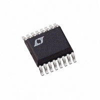
LTC2435CGN Linear Technology, LTC2435CGN Datasheet - Page 14

LTC2435CGN
Manufacturer Part Number
LTC2435CGN
Description
IC ADC DIFF I/REF 20BIT 16-SSOP
Manufacturer
Linear Technology
Datasheet
1.LTC2435-1CGN.pdf
(40 pages)
Specifications of LTC2435CGN
Number Of Bits
20
Sampling Rate (per Second)
15
Data Interface
MICROWIRE™, Serial, SPI™
Number Of Converters
2
Power Dissipation (max)
1mW
Voltage Supply Source
Single Supply
Operating Temperature
0°C ~ 70°C
Mounting Type
Surface Mount
Package / Case
16-SSOP (0.150", 3.90mm Width)
Lead Free Status / RoHS Status
Contains lead / RoHS non-compliant
Available stocks
Company
Part Number
Manufacturer
Quantity
Price
Company:
Part Number:
LTC2435CGN
Manufacturer:
LT
Quantity:
10 000
Part Number:
LTC2435CGN
Manufacturer:
LTNEAR
Quantity:
20 000
Part Number:
LTC2435CGN#PBF
Manufacturer:
LINEAR/凌特
Quantity:
20 000
APPLICATIO S I FOR ATIO
LTC2435/LTC2435-1
Output Data Format
The LTC2435/LTC2435-1 serial output data stream is 24
bits long. The first 3 bits represent status information
indicating the sign and conversion state. The next 21 bits
are the conversion result, MSB first. The third and fourth
bit together are also used to indicate an underrange
condition (the differential input voltage is below –FS) or an
overrange condition (the differential input voltage is above
+FS).
Bit 23 (first output bit) is the end of conversion (EOC)
indicator. This bit is available at the SDO pin during the
conversion and sleep states whenever the CS pin is LOW.
This bit is HIGH during the conversion and goes LOW
when the conversion is complete.
Bit 22 (second output bit) is a dummy bit (DMY) and is
always LOW.
Bit 21 (third output bit) is the conversion result sign indi-
cator (SIG). If V
bit is LOW.
Bit 20 (fourth output bit) is the most significant bit (MSB)
of the result. This bit in conjunction with Bit 21 also
provides the underrange or overrange indication. If both
Bit 21 and Bit 20 are HIGH, the differential input voltage is
above +FS. If both are LOW, the differential input voltage
is below –FS.
The function of these bits is summarized in Table 1.
Table 1. LTC2435/LTC2435-1 Status Bits
Input Range
V
0V ≤ V
–0.5 • V
V
Bits 20-0 are the 21-bit conversion result MSB first.
Bit 0 is the least significant bit (LSB).
Data is shifted out of the SDO pin under control of the serial
clock (SCK), see Figure 3. Whenever CS is HIGH, SDO
remains high impedance and any externally generated
14
IN
IN
≥ 0.5 • V
< – 0.5 • V
IN
REF
< 0.5 • V
≤ V
REF
REF
IN
REF
< 0V
IN
is >0, this bit is HIGH. If V
U
U
Bit 23 Bit 22 Bit 21 Bit 20
EOC
0
0
0
0
W
DMY
0
0
0
0
IN
SIG
is <0, this
U
1
1
0
0
MSB
1
0
1
0
SCK clock pulses are ignored by the internal data out shift
register.
In order to shift the conversion result out of the device, CS
must first be driven LOW. EOC is seen at the SDO pin of the
device once CS is pulled LOW. EOC changes real time from
HIGH to LOW at the completion of a conversion. This
signal may be used as an interrupt for an external
microcontroller. Bit 23 (EOC) can be captured on the first
rising edge of SCK. Bit 22 is shifted out of the device on the
first falling edge of SCK. The final data bit (Bit 0) is shifted
out on the falling edge of the 23rd SCK and may be latched
on the rising edge of the 24th SCK pulse. On the falling
edge of the 24th SCK pulse, SDO goes HIGH indicating the
initiation of a new conversion cycle. This bit serves as EOC
(Bit 23) for the next conversion cycle. Table 2 summarizes
the output data format.
As long as the voltage on the IN
within the – 0.3V to (V
operating range, a conversion result is generated for any
differential input voltage V
+FS = 0.5 • V
than +FS, the conversion result is clamped to the value
corresponding to the +FS. For differential input voltages
below –FS, the conversion result is clamped to the value
corresponding to –FS – 1LSB.
Offset Accuracy and Drift
Unlike the LTC2430 and most of the LTC2400 family, the
LTC2435/LTC2435-1 do not perform an offset calibration
every cycle. The reason for this is to increase the data output
rate while maintaining line frequency rejection.
While the initial accuracy of the LTC2435/LTC2435-1
offset is within 5mV (see Figure 4), several unique prop-
erties of the LTC2435/LTC2435-1 architecture nearly elimi-
nate the drift of the offset error with respect to temperature
and supply.
As shown in Figure 5, the offset variation with temperature
is less than 3ppm over the complete temperature range of
–50°C to 100°C. This corresponds to a temperature drift
of 0.022ppm/°C.
While the variation in offset with supply voltage is propor-
REF
. For differential input voltages greater
CC
IN
+ 0.3V) absolute maximum
from –FS = –0.5 • V
+
and IN
–
pins is maintained
REF
24351fb
to


