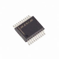
MAX1135BEAP+ Maxim Integrated Products, MAX1135BEAP+ Datasheet - Page 10

MAX1135BEAP+
Manufacturer Part Number
MAX1135BEAP+
Description
IC ADC 16BIT 150KSPS 20-SSOP
Manufacturer
Maxim Integrated Products
Datasheet
1.MAX1134BEAP.pdf
(18 pages)
Specifications of MAX1135BEAP+
Number Of Bits
16
Sampling Rate (per Second)
150k
Data Interface
MICROWIRE™, QSPI™, Serial, SPI™
Number Of Converters
1
Power Dissipation (max)
26.4mW
Voltage Supply Source
Analog and Digital
Operating Temperature
-40°C ~ 85°C
Mounting Type
Surface Mount
Package / Case
20-SSOP
Number Of Adc Inputs
1
Architecture
SAR
Conversion Rate
150 KSPs
Resolution
16 bit
Interface Type
Serial
Voltage Reference
External
Supply Voltage (max)
3.3 V
Mounting Style
SMD/SMT
Input Voltage
2.048 V
Lead Free Status / RoHS Status
Lead free / RoHS Compliant
The user-programmable outputs are set to zero during
power-on reset or when RST goes low. During hardware
or software shutdown, P0, P1, and P2 are unchanged
and remain low impedance.
Start a conversion by clocking a control byte into the
device’s internal shift register. With CS low, each rising
edge on SCLK clocks a bit from DIN into the
MAX1134/MAX1135s’ internal shift register. After CS
goes low or after a conversion or calibration completes,
the first arriving logic 1 is defined as the start bit of the
control byte. Until this first start bit arrives, any number of
logic 0 bits can be clocked into DIN with no effect. If at
any time during acquisition or conversion CS is brought
high and then low again, the part is placed into a state
where it can recognize a new start bit. If a new start bit
occurs before the current conversion is complete, the
conversion is aborted and a new acquisition is initiated.
Figure 4. External Clock Mode SSTRB Detailed Timing
16-Bit ADCs, 150ksps, 3.3V Single Supply
Figure 3. Long Acquisition Mode (32 Clock Cycles) External Clock
10
SSTRB
______________________________________________________________________________________
DOUT
SCLK
DIN
STATE
CS
A/D
SSTRB
SCLK
START
IDLE
CS
1
UNI/
BIP
INT/
EXT
t
ACQ
M1
Starting a Conversion
4
M0
t
SDV
ACQUISITION
P2
P1
P0
8
P1 CLOCKED IN
14
15
The MAX1134/MAX1135 use either the external serial
clock or the internal clock to perform the successive-
approximation conversion. In both clock modes, the
external clock shifts data in and out of the
MAX1134/MAX1135. Bit 5 (INT/EXT) of the control byte
programs the clock mode.
In external clock mode, the external clock not only
shifts data in and out, but also drives the ADC conver-
sion steps.
In short acquisition mode, SSTRB pulses high for one
clock period after the seventh falling edge of SCLK fol-
lowing the start bit. The MSB of the conversion is avail-
able at DOUT on the eighth falling edge of SCLK
(Figure 2).
MSB
B15
t
SSTRB
B14
B13
Internal and External Clock Modes
CONVERSION
B4
t
SSTRB
B3
29
B2
B1
LSB
B0
32
t
FILLED WITH
STR
ZEROS
External Clock
IDLE


