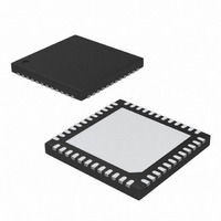
MAX19517ETM+ Maxim Integrated Products, MAX19517ETM+ Datasheet - Page 33

MAX19517ETM+
Manufacturer Part Number
MAX19517ETM+
Description
IC ADC 10BIT 130MSPS DUAL 48TQFN
Manufacturer
Maxim Integrated Products
Datasheet
1.MAX19517ETM.pdf
(35 pages)
Specifications of MAX19517ETM+
Number Of Bits
10
Sampling Rate (per Second)
130M
Data Interface
Serial, Parallel
Number Of Converters
2
Voltage Supply Source
Analog and Digital
Operating Temperature
-40°C ~ 85°C
Mounting Type
Surface Mount
Package / Case
48-TQFN Exposed Pad
Conversion Rate
130 MSPs
Resolution
10 bit
Interface Type
SPI
Snr
59.9 dB
Voltage Reference
1.25 V
Supply Voltage (max)
3.5 V
Supply Voltage (min)
1.7 V
Maximum Power Dissipation
3200 mW
Maximum Operating Temperature
+ 85 C
Mounting Style
SMD/SMT
Input Voltage
1.8 V
Minimum Operating Temperature
- 40 C
Lead Free Status / RoHS Status
Lead free / RoHS Compliant
SSNF is the integrated noise and distortion power in the
Nyquist band for small-signal inputs. The DC offset is
excluded from this noise calculation. For this converter, a
small signal is defined as a single tone with an amplitude
less than -35dBFS. This parameter captures the thermal
and quantization noise characteristics of the converter
and can be used to help calculate the overall noise figure
of a receive channel. Refer to
application notes on Thermal + Quantization Noise Floor.
For a waveform perfectly reconstructed from digital
samples, the theoretical maximum SNR is the ratio of
the full-scale analog input (RMS value) to the RMS
quantization error (residual error). The ideal, theoretical
minimum analog-to-digital noise is caused by quantiza-
tion error only and results directly from the ADC’s reso-
lution (N bits):
In reality, there are other noise sources besides quanti-
zation noise (e.g., thermal noise, reference noise, clock
jitter, etc.). SNR is computed by taking the ratio of the
RMS signal to the RMS noise. RMS noise includes all
spectral components to the Nyquist frequency exclud-
ing the fundamental, the first six harmonics (HD2–HD7),
and the DC offset.
SINAD is computed by taking the ratio of the RMS sig-
nal to the RMS noise plus the RMS distortion. RMS
noise includes all spectral components to the Nyquist
frequency excluding the fundamental, the first six har-
monics (HD2–HD7), and the DC offset. RMS distortion
includes the first six harmonics (HD2–HD7).
SINAD
Signal-to-Noise and Distortion (SINAD)
SNR
=
20
SNR
=
×
Small-Signal Noise Floor (SSNF)
log
20
______________________________________________________________________________________
[max]
⎛
⎜
⎜
⎝
Signal-to-Noise Ratio (SNR)
×
NOISE
log
= 6.02 x N + 1.76
⎛
⎜
⎝
SIGNAL
RMS
NOISE
Dual-Channel, 10-Bit, 130Msps ADC
www.maxim-ic.com
SIGNAL
2
+
RMS
DISTORTION
RMS
RMS
⎞
⎟
⎠
RMS
2
⎞
⎟
⎟
⎠
for
SFDR is the ratio expressed in decibels of the RMS
amplitude of the fundamental (maximum signal compo-
nent) to the RMS amplitude of the next largest spurious
component, excluding DC offset. SFDR1 reflects the
spurious performance based on worst 2nd-order or
3rd-order harmonic distortion. SFDR2 is defined by the
worst spurious component excluding 2nd- and 3rd-
order harmonics and DC offset.
THD is the ratio of the RMS of the first six harmonics of
the input signal to the fundamental itself. This is
expressed as:
where V
the amplitudes of the 2nd-order through 7th-order har-
monics (HD2–HD7).
IM3 is the total power of the third-order intermodulation
products to the Nyquist frequency relative to the total
input power of the two input tones f
individual input tone levels are at -7dBFS. The third-
order intermodulation products are: 2 x f
f
The input signal is sampled on the rising edge of the
sampling clock. There is a small delay between the ris-
ing edge of the sampling clock and the actual sampling
instant, which is defined as aperture delay (t
Aperture jitter (t
time variation in the aperture delay.
Overdrive recovery time is the time required for the
ADC to recover from an input transient that exceeds the
full-scale limits. The specified overdrive recovery time is
measured with an input transient that exceeds the full-
scale limits by ±10%.
PROCESS: CMOS
IN2
Single-Tone Spurious-Free Dynamic Range
THD
- f
IN1
=
1
, 2 x f
20
is the fundamental amplitude and V
Third-Order Intermodulation (IM3)
×
Total Harmonic Distortion (THD)
log
IN1
AJ
⎛
⎜
⎜
⎝
) is defined as the sample-to-sample
+ f
V
2
IN2
2
Overdrive Recovery Time
+
, 2 x f
V
3
2
Chip Information
+
IN2
(SFDR1 and SFDR2)
V
4
2
+ f
V
+
1
IN1
Aperture Delay
Aperture Jitter
V
IN1
5
2
.
+
and f
IN1
V
6
AD
2
- f
+
).
2
IN2
IN2
–V
V
7
2
. The
7
, 2 x
⎞
⎟
⎟
⎠
are
33


