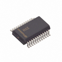
MAX1296AEEG+ Maxim Integrated Products, MAX1296AEEG+ Datasheet

MAX1296AEEG+
Specifications of MAX1296AEEG+
Related parts for MAX1296AEEG+
MAX1296AEEG+ Summary of contents
Page 1
... QSOP MAX1296AEEG -40°C to +85°C 24 QSOP MAX1296BEEG -40°C to +85°C 24 QSOP ________________________________________________________________ Maxim Integrated Products For pricing, delivery, and ordering information, please contact Maxim/Dallas Direct! at 1-888-629-4642, or visit Maxim’s website at www.maxim-ic.com. o 12-Bit Resolution, ±0.5 LSB Linearity o Single +5V Operation o Internal +2.5V Reference ...
Page 2
ADCs with +2.5V Reference and Parallel Interface ABSOLUTE MAXIMUM RATINGS V to GND ..............................................................-0.3V to +6V DD CH0–CH5, COM to GND ............................-0. REF, REFADJ to GND.................................-0. Digital Inputs to GND ...............................................-0.3V to ...
Page 3
ADCs with +2.5V Reference and Parallel Interface ELECTRICAL CHARACTERISTICS (continued +5V ±10%, COM = GND, REFADJ = unless otherwise noted. Typical values are ...
Page 4
ADCs with +2.5V Reference and Parallel Interface TIMING CHARACTERISTICS (V = +5V ±10%, COM = GND, REFADJ = unless otherwise noted. Typical values are MIN ...
Page 5
ADCs with +2.5V Reference and Parallel Interface (V = +5V +2.500V 7.6MHz REF CLK INTEGRAL NONLINEARITY vs. DIGITAL OUTPUT CODE 0.5 0.4 0.3 0.2 0.1 0 -0.1 -0.2 -0.3 -0.4 ...
Page 6
ADCs with +2.5V Reference and Parallel Interface (V = +5V +2.500V 7.6MHz REF CLK INTERNAL REFERENCE VOLTAGE vs. SUPPLY VOLTAGE 2.53 2.52 2.51 2.50 2.49 2.48 4.50 4.75 5.00 5.25 ...
Page 7
ADCs with +2.5V Reference and Parallel Interface PIN NAME MAX1294 MAX1296 ...
Page 8
ADCs with +2.5V Reference and Parallel Interface PIN NAME MAX1294 MAX1296 25 21 REF D11 28 24 D10 (CH5) (CH4) ANALOG INPUT (CH3) MULTIPLEXER (CH2) CH1 CH0 COM CLK CLOCK ...
Page 9
ADCs with +2.5V Reference and Parallel Interface Single-Ended and Pseudo-Differential Operation The sampling architecture of the ADCs’ analog com- parator is illustrated in the equivalent input circuits of Figure 3. In single-ended mode, IN+ is internally ...
Page 10
ADCs with +2.5V Reference and Parallel Interface Table 2. Channel Selection for Single-Ended Operation (SGL/DIF = ...
Page 11
ADCs with +2.5V Reference and Parallel Interface the acquisition time lengthens and more time must be allowed between conversions. The acquisition time the maximum time the device takes to acquire ACQ the signal, ...
Page 12
ADCs with +2.5V Reference and Parallel Interface CSWS CONTROL D7–D0 BYTE ACQMOD = "0" HIGH-Z INT RD HIGH-Z DOUT Figure 4. Conversion Timing Using Internal Acquisition Mode ...
Page 13
ADCs with +2.5V Reference and Parallel Interface External Clock Mode To select external clock mode, bits D6 and D7 of the control byte must be set to 1. Figure 6 shows the clock and WR timing ...
Page 14
ADCs with +2.5V Reference and Parallel Interface Table 4. Control-Byte Format (MSB) PD1 PD0 ACQMOD The control bit sequence is latched into the device on pins D7–D0 during a write command. Table 4 ...
Page 15
ADCs with +2.5V Reference and Parallel Interface Table 5. Full Scale and Zero Scale for Unipolar and Bipolar Operation UNIPOLAR MODE Full Scale Zero Scale — OUTPUT CODE FULL-SCALE TRANSITION FS = REF + COM 111 ...
Page 16
ADCs with +2.5V Reference and Parallel Interface CLK WR RD CONTROL D11– D7–D0 WORD D0 STATE ACQUISITION SAMPLING INSTANT Figure 10. Timing Diagram for Fastest Conversion tion or conversion can cause ...
Page 17
ADCs with +2.5V Reference and Parallel Interface Integral Nonlinearity Integral nonlinearity (INL) is the deviation of the values on an actual transfer function from a straight line. This straight line can be either a best-straight-line fit ...
Page 18
ADCs with +2.5V Reference and Parallel Interface CLK MAX1294 REF µP CONTROL WR REFADJ INPUTS RD INT D11 D10 CH5 D6 CH4 D5 CH3 D4 CH2 D3 CH1 D2 CH0 ...
Page 19
... Maxim cannot assume responsibility for use of any circuitry other than circuitry entirely embodied in a Maxim product. No circuit patent licenses are implied. Maxim reserves the right to change the circuitry and specifications without notice at any time. Maxim Integrated Products, 120 San Gabriel Drive, Sunnyvale, CA 94086 408-737-7600 _____________________19 © 2002 Maxim Integrated Products Printed USA is a registered trademark of Maxim Integrated Products ...


