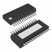
MAX1261BCEI+ Maxim Integrated Products, MAX1261BCEI+ Datasheet - Page 18

MAX1261BCEI+
Manufacturer Part Number
MAX1261BCEI+
Description
IC ADC 12-BIT 250KSPS 28-QSOP
Manufacturer
Maxim Integrated Products
Datasheet
1.MAX1263BCEG.pdf
(20 pages)
Specifications of MAX1261BCEI+
Number Of Bits
12
Sampling Rate (per Second)
250k
Data Interface
Parallel
Number Of Converters
1
Power Dissipation (max)
5.1mW
Voltage Supply Source
Single Supply
Operating Temperature
0°C ~ 70°C
Mounting Type
Surface Mount
Package / Case
28-QSOP
Lead Free Status / RoHS Status
Lead free / RoHS Compliant
250ksps, +3V, 8-/4-Channel, 12-Bit ADCs
with +2.5V Reference and Parallel Interface
Figure 10. Timing Diagram for Fastest Conversion
Effective number of bits (ENOB) indicates the global
accuracy of an ADC at a specific input frequency and
sampling rate. An ideal ADC error consists of quantiza-
tion noise only. With an input range equal to the full-
scale range of the ADC, calculate the effective number
of bits as follows:
Total harmonic distortion (THD) is the ratio of the RMS
sum of the first five harmonics of the input signal to the
fundamental itself. This is expressed as:
where V
V
monics.
Spurious-free dynamic range (SFDR) is the ratio of the
RMS amplitude of the fundamental (maximum signal
component) to the RMS value of the next-largest distor-
tion component.
18
THD
5
are the amplitudes of the 2nd- through 5th-order har-
D7–D0
STATE
HBEN
______________________________________________________________________________________
CLK
WR
RD
=
1
CONTROL
20
is the fundamental amplitude, and V
BYTE
ENOB = (SINAD - 1.76) / 6.02
x
1
log
Spurious-Free Dynamic Range
ACQUISITION
D7–D0 D11–D8
2
LOW
BYTE
Total Harmonic Distortion
V
2
3
Effective Number of Bits
HIGH
2
BYTE
SAMPLING INSTANT
+
4
V
3
2
5
+
V
4
2
6
+
V
7
5
2
2
through
8
/
V
1
9
CONTROL BYTE
CONVERSION
10
Figure 11. Power-Supply and Grounding Connections
TRANSISTOR COUNT: 5781
SUBSTRATE CONNECTED TO GND
R* = 5Ω
11
*OPTIONAL
V
+3V
DD
12
4.7µF
0.1µF
13
MAX1261
MAX1263
14
GND
15
SUPPLIES
16
Chip Information
COM
V
LOGIC
D7–D0 D11–D8
LOW
BYTE
= +2V/+3V GND
+2V/+3V
ACQUISITION
CIRCUITRY
DIGITAL
HIGH
BYTE
DGND


