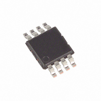
MAX157BEUA+ Maxim Integrated Products, MAX157BEUA+ Datasheet - Page 12

MAX157BEUA+
Manufacturer Part Number
MAX157BEUA+
Description
IC ADC 10BIT 108KSPS 2CH 8-UMAX
Manufacturer
Maxim Integrated Products
Datasheet
1.MAX157BEUA.pdf
(16 pages)
Specifications of MAX157BEUA+
Number Of Bits
10
Sampling Rate (per Second)
108k
Data Interface
MICROWIRE™, QSPI™, Serial, SPI™
Number Of Converters
1
Power Dissipation (max)
330mW
Voltage Supply Source
Single Supply
Operating Temperature
-40°C ~ 85°C
Mounting Type
Surface Mount
Package / Case
8-TSSOP, 8-MSOP (0.118", 3.00mm Width)
Lead Free Status / RoHS Status
Lead free / RoHS Compliant
Using the high-speed QSPI interface with CPOL = 0
and CPHA = 0, the MAX157/MAX159 supports a maxi-
mum f
can be programmed to perform a conversion on each
of the two channels for the MAX157.
Figure 9b shows the QSPI interface timing.
The MAX157/MAX159 are compatible with a PIC16/
PIC17 microcontroller (µC), using the synchronous seri-
al port (SSP) module.
To establish SPI communication, connect the controller
as shown in Figure 10a and configure the PIC16/PIC17
as system master by initializing its synchronous serial
port control register (SSPCON) and synchronous serial
port status register (SSPSTAT) to the bit patterns shown
in Tables 2 and 3.
In SPI mode, the PIC16/PIC17 µCs allow eight bits of
data to be synchronously transmitted and received
simultaneously. Two consecutive 8-bit readings (Figure
10b) are necessary to obtain the entire 10-bit result
from the ADC. DOUT data transitions on the serial
clock’s falling edge and is clocked into the µC on
SCLK’s rising edge. The first 8-bit data stream contains
+2.7V, Low-Power, 2-Channel,
108ksps, Serial 10-Bit ADCs in 8-Pin µMAX
Figure 8a. SPI Connections
Figure 8c. SPI/MICROWIRE Interface Timing Sequence (CPOL = CPHA = 0)
12
*WHEN CS/SHDN IS HIGH, DOUT = HIGH -Z
CS/SHDN
______________________________________________________________________________________
DOUT*
SCLK
SCLK
SPI
of 2.17MHz. The QSPI circuit in Figure 9a
MISO
SCK
I/O
SS
V
PIC16 with SSP Module
DD
1
SAMPLING
and PIC17 Interface
INSTANT
2
3
CS/SHDN
SCLK
DOUT
QSPI Interface
CHID
1ST BYTE READ
MAX157
MAX159
4
MSB
D9
5
D8
6
D7
7
D6
8
three leading ones, the channel identification, and the
first four data bits starting with the MSB. The second 8-
bit data stream contains the remaining bits, D5 through
D0, and the two sub-bits S1 and S0.
For best performance use printed circuit boards
(PCBs), wire-wrap configurations are not recommend-
ed, since the layout should ensure proper separation of
analog and digital traces. Run analog and digital lines
anti-parallel to each other, and don’t layout digital sig-
nal paths underneath the ADC package. Use separate
analog and digital PCB ground sections with only one
Figure 8b. MICROWIRE Connections
Figure 9a. QSPI Connections
D5
MICROWIRE
QSPI
Layout, Grounding, and Bypassing
9
MISO
SCK
D4
CS
SS
I/O
10
SK
SI
D3
11
2ND BYTE READ
V
D2
DD
12
D1
13
LSB
D0
14
CS/SHDN
SCLK
DOUT
CS/SHDN
SCLK
DOUT
S1
15
MAX157
MAX159
MAX157
MAX159
S0
16
HIGH-Z


