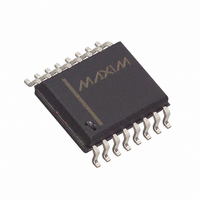
MAX1415EWE+ Maxim Integrated Products, MAX1415EWE+ Datasheet - Page 28

MAX1415EWE+
Manufacturer Part Number
MAX1415EWE+
Description
IC ADC 16BIT DELTA SIGMA 16-SOIC
Manufacturer
Maxim Integrated Products
Datasheet
1.MAX1415EUE.pdf
(36 pages)
Specifications of MAX1415EWE+
Number Of Bits
16
Sampling Rate (per Second)
500
Data Interface
MICROWIRE™, QSPI™, Serial, SPI™
Number Of Converters
1
Power Dissipation (max)
762mW
Voltage Supply Source
Single Supply
Operating Temperature
-45°C ~ 85°C
Mounting Type
Surface Mount
Package / Case
16-SOIC (0.300", 7.50mm Width)
Lead Free Status / RoHS Status
Lead free / RoHS Compliant
Write to the calibration registers in normal mode only.
After writing to the calibration registers, the devices
implement the new offset and gain-register calibration
coefficients at the beginning of a new acquisition. To
ensure the results are valid, discard the first conversion
result after writing to the calibration registers.
To ensure that a conversion is not made using invalid
calibration data, drive FSYNC high prior to writing to the
calibration registers, and then release FSYNC low to ini-
tiate conversion.
At power-up, the serial interface, logic, digital filter, and
modulator circuits are reset. The registers are set to their
default values. The device returns to wait for a write to
the communications register. For accurate measure-
ments, perform calibration routines after power-up. Allow
time for the external reference and internal or external
oscillator to start up before starting calibration. See the
Typical Operating Characteristics for typical internal and
external oscillator startup times.
Drive RESET low to reset the MAX1415/MAX1416 to
power-on reset status. DRDY goes high and all communi-
cation to the MAX1415/MAX1416 is ignored while RESET
is low. Upon releasing RESET, the device must be recon-
figured to begin a conversion. The device returns to wait-
ing for a write to the communication register after a reset
has been performed. Perform a calibration sequence fol-
lowing a reset for accurate conversions.
When using an external clock or crystal oscillator, the
MAX1415/MAX1416 clock generator continues to run
when RESET is pulled low. This allows any device run-
ning from CLKOUT to be uninterrupted when the device
is in reset while using an external clock.
The recommended frequency range of the external
clock is 400kHz to 2.5MHz (clkdw = 0). The output data
rate and first notch frequency are dependent on the
decimation rate of the digital filter.
available decimation rates of the digital filter. The out-
put data rate and filter first notch is calculated using the
following formula:
(if CLKDIV = 1).
16-Bit, Low-Power, 2-Channel,
Sigma-Delta ADCs
28
Output data rate
Selecting Custom Output Data Rates and
______________________________________________________________________________________
=
128
×
First Notch Frequency
Decimation Rate
f
CLKIN
Power-On Reset
Table 14 shows the
×
Reset
0 5
.
(if CLKDIV = 0).
Note: First notch filter frequency = output data rate.
At power-on reset, the MAX1415/MAX1416 expect a
write to the communications register. Writing to the
communications register selects the acquisition chan-
nel, read/write operation for the next register, power-
down/normal mode, and the address of the following
register to be accessed. The MAX1415/MAX1416 have
six user-accessible registers, which control the function
of the device and allow the result to be read. Write to
the communications register before accessing any
other registers.
Writing to the clock and setup registers after configuring
and initializing the host processor serial port sets up the
MAX1415/MAX1416. Use self- or system calibrations to
minimize offset and gain errors (see the Calibration sec-
tion for more details). Set FSYNC = 0 to begin calibration
or conversion. The MAX1415/MAX1416 perform free-run-
ning acquisitions when FSYNC is low (see the Using
FSYNC section). The µC can poll the DRDY bit of the
communications register and read the data register
when the DRDY bit returns a 0. For hardware polling, the
DRDY output goes low when the new data is valid in the
data register.
The data register can be read multiple times while the
next conversion takes place.
The flow diagram in Figure 11 shows an example
sequence required to perform a conversion on channel
1 (AIN1+/AIN1-) after a power-on reset.
Table 14. Filter Select and Decimation
Rate
CLK
0
0
0
0
1
1
1
1
Output data rate
FS1
0
0
1
1
0
0
1
1
=
Performing a Conversion
128
FS0
0
1
0
1
0
1
0
1
×
Decimation Rate
f
CLKIN
DECIMATION RATE
391
313
384
320
78
39
77
38


