LM97593VH/NOPB National Semiconductor, LM97593VH/NOPB Datasheet - Page 10
LM97593VH/NOPB
Manufacturer Part Number
LM97593VH/NOPB
Description
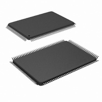
IC DDC ADC/TUNER/AGC 128-PQFP
Manufacturer
National Semiconductor
Datasheet
1.LM97593VHNOPB.pdf
(50 pages)
Specifications of LM97593VH/NOPB
Number Of Bits
12
Sampling Rate (per Second)
65M
Data Interface
Serial
Number Of Converters
2
Power Dissipation (max)
560mW
Voltage Supply Source
Analog and Digital
Operating Temperature
-40°C ~ 85°C
Mounting Type
Surface Mount
Package / Case
128-BFQFP
Lead Free Status / RoHS Status
Lead free / RoHS Compliant
Other names
LM97593VH
Available stocks
Company
Part Number
Manufacturer
Quantity
Price
Company:

Part Number:
LM97593VH/NOPB
Manufacturer:
VK
Quantity:
1 980
Company:
Part Number:
LM97593VH/NOPB
Manufacturer:
Texas Instruments
Quantity:
10 000


www.national.com
t
JTAG
Microprocessor Interface
t
t
t
t
t
JCL
CSU
CHD
CSPW
CDLY
CZ
Note 1: Absolute Maximum Ratings indicate limits beyond which damage to the device may occur. Operating Ratings indicate conditions for which the device is
guaranteed to be functional, but do not guarantee specific performance limits. For guaranteed specifications and test conditions, see the Electrical Characteristics.
The guaranteed specifications apply only for the test conditions listed. Some performance characteristics may degrade when the device is not operated under
the listed test conditions. Operation of the device beyond the maximum Operating Ratings is not recommended.
Note 2: All voltages are measured with respect to GND = AGND = DGND = DRGND = 0V, unless otherwise specified.
Note 3: When the input voltage at any pin exceeds the power supplies (that is, V
±50 mA maximum package input current rating limits the number of pins that can safely exceed the power supplies with an input current of ±25 mA to two.
Note 4: The maximum allowable power dissipation is dictated by T
can be calculated using the formula P
operated in a severe fault condition (e.g. when input or output pins are driven beyond the power supply voltages, or the power supply polarity is reversed). Such
conditions should always be avoided.
Note 5: Human Body Model is 100 pF discharged through a 1.5 kΩ resistor. Machine Model is 220 pF discharged through 0 Ω.
Note 6: Reflow temperature profiles are different for lead-free and non-lead-free packages.
Note 7: The inputs are protected as shown below. Input voltage magnitudes above V
(Note 3)
Note 8: To guarantee accuracy, it is required that |V
Note 9: With the test condition for V
Note 10: Typical figures are at T
guaranteed. Test Limits are guaranteed to National's AOQL (Average Outgoing Quality Level).
Note 11: Integral Non Linearity is defined as the deviation of the analog value, expressed in LSBs, from the straight line that passes through positive and negative
full-scale.
Note 12: The input capacitance is the sum of the package/pin capacitance and the sample and hold circuit capacitance.
Note 13: Timing specifications are tested at TTL logic levels, V
Note 14: Optimum performance will be obtained by keeping the reference input in the 0.8V to 1.2V range. The LM4051CIM3-ADJ (SOT23 package) is
recommended for external reference applications.
Note 15: I
V
supply voltage, C
Note 16: (+x) indicates the additional dynamic range provided by the AGC. The DVGA in front of the LM97593 provides 42 dB of gain adjustment.
Symbol
DR
, and the rate at which the outputs are switching (which is signal dependent). I
FMAX
.
DR
is the current consumed by the switching of the output drivers and is primarily determined by load capacitance on the output pins, the supply voltage,
TCK Pulse Width Low (Figure 14)
TCK Maximum Frequency (Figure 14)
Control Setup before the controlling signal goes low (Figure 15)
Control hold after the controlling signal goes high (Figure 15)
Controlling strobe pulse width (Write) (Figure 15)
Control output delay controlling signal low to D (Read) (Figure 15)
Control tri-state delay after controlling signal high (Figure 15)
n
is total capacitance on the output pin, and f
A
= 25°C and represent most likely parametric norms at the time of product characterization. The typical specifications are not
REF
D,max
= +1.0V (2V
= (T
Parameter (C
J,max
- T
P-P
A
–V
A
differential input), the 12-Bit LSB is 488 µV.
D
)/θ
|
≤
JA
100 mV and separate bypass capacitors are used at each power supply pin.
. The values for maximum power dissipation listed above will be reached only when the device is
n
IL
is the average frequency at which that pin is toggling.
L
= 0.4V for a falling edge and V
=50pF)
J,max
, the junction-to-ambient thermal resistance, (θ
10
IN
DR
< AGND, or V
=V
A
or below GND will not damage this device, provided current is limited per
DR
(C
30008770
0
x f
IH
0
IN
+ C
= 2.4V for a rising edge.
> V
1
A
x f
), the current at that pin should be limited to ±25 mA. The
1
+....C
Min
40
30
5
5
11
x f
JA
11
), and the ambient temperature, (T
) where V
Typical
(Note
10)
DR
is the output driver power
Max
10
30
20
Units
MHz
ns
ns
ns
ns
ns
ns
A
), and
Related parts for LM97593VH/NOPB
Image
Part Number
Description
Manufacturer
Datasheet
Request
R

Part Number:
Description:
12BIT ADC, 2CH, DDC/AGC, 128PQFP
Manufacturer:
National Semiconductor
Datasheet:

Part Number:
Description:
Manufacturer:
National Semiconductor
Datasheet:
Part Number:
Description:
National Semiconductor [8-Bit D/A Converter]
Manufacturer:
National Semiconductor
Datasheet:
Part Number:
Description:
National Semiconductor [Media Coprocessor]
Manufacturer:
National Semiconductor
Datasheet:
Part Number:
Description:
Digitally Controlled Tone and Volume Circuit with Stereo Audio Power Amplifier, Microphone Preamp Stage and National 3D Sound
Manufacturer:
National Semiconductor
Datasheet:
Part Number:
Description:
Digitally Controlled Tone and Volume Circuit with Stereo Audio Power Amplifier, Microphone Preamp Stage and National 3D Sound
Manufacturer:
National Semiconductor
Datasheet:
Part Number:
Description:
AC97 Rev 2 Codec with Sample Rate Conversion and National 3D Sound
Manufacturer:
National Semiconductor
Part Number:
Description:
Manufacturer:
National Semiconductor
Datasheet:
Part Number:
Description:
Manufacturer:
National Semiconductor
Datasheet:
Part Number:
Description:
General Purpose, Low Voltage, Low Power, Rail-to-Rail Output Operational Amplifiers
Manufacturer:
National Semiconductor
Datasheet:
Part Number:
Description:
8-bit 20 MSPS flash A/D converter.
Manufacturer:
National Semiconductor
Datasheet:
Part Number:
Description:
Low Noise Quad Operational Amplifier
Manufacturer:
National Semiconductor
Datasheet:
Part Number:
Description:
Quad Differential Line Receivers
Manufacturer:
National Semiconductor
Datasheet:
Part Number:
Description:
Quad High Speed Trapezoidal? Bus Transceiver
Manufacturer:
National Semiconductor
Datasheet: