AD574AKD Analog Devices Inc, AD574AKD Datasheet - Page 5
AD574AKD
Manufacturer Part Number
AD574AKD
Description
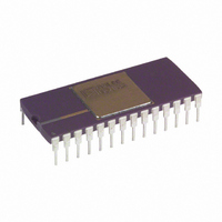
IC ADC 12BIT W/REF 28-CDIP
Manufacturer
Analog Devices Inc
Specifications of AD574AKD
Data Interface
Parallel
Rohs Status
RoHS non-compliant
Number Of Bits
12
Sampling Rate (per Second)
28.6k
Number Of Converters
1
Power Dissipation (max)
725mW
Voltage Supply Source
Dual ±
Operating Temperature
0°C ~ 70°C
Mounting Type
Through Hole
Package / Case
28-CDIP (0.600", 15.24mm)
Resolution (bits)
12bit
Input Channel Type
Differential
Supply Voltage Range - Analogue
± 11.4V To ± 16.5V
Supply Voltage Range - Digital
4.5V To 5.5V
Supply Current
30mA
No.
RoHS Compliant
Digital Ic Case Style
DIP
No. Of Pins
28
Rohs Compliant
No
Lead Free Status / RoHS Status
Available stocks
Company
Part Number
Manufacturer
Quantity
Price
Company:

Part Number:
AD574AKD
Manufacturer:
INTERSIL
Quantity:
210
Company:
Part Number:
AD574AKD
Manufacturer:
AD
Quantity:
3 909
Company:
Part Number:
AD574AKD
Manufacturer:
AD
Quantity:
3 909
Part Number:
AD574AKD
Manufacturer:
ADI/亚德诺
Quantity:
20 000
Company:
Part Number:
AD574AKD/AJD
Manufacturer:
MOT
Quantity:
4


THE AD574A OFFERS GUARANTEED MAXIMUM LINEARITY ERROR OVER THE FULL OPERATING
TEMPERATURE RANGE
REV. B
DEFINITIONS OF SPECIFICATIONS
LINEARITY ERROR
Linearity error refers to the deviation of each individual code
from a line drawn from “zero” through “full scale”. The point
used as “zero” occurs 1/2 LSB (1.22 mV for 10 volt span) be-
fore the first code transition (all zeros to only the LSB “on”).
“Full scale” is defined as a level 1 1/2 LSB beyond the last code
transition (to all ones). The deviation of a code from the true
straight line is measured from the middle of each particular
code.
The AD574AK, L, T, and U grades are guaranteed for maxi-
mum nonlinearity of 1/2 LSB. For these grades, this means
that an analog value which falls exactly in the center of a given
code width will result in the correct digital output code. Values
nearer the upper or lower transition of the code width may pro-
duce the next upper or lower digital output code. The AD574AJ
and S grades are guaranteed to 1 LSB max error. For these
grades, an analog value which falls within a given code width
will result in either the correct code for that region or either
adjacent one.
Note that the linearity error is not user-adjustable.
DIFFERENTIAL LINEARITY ERROR (NO MISSING
CODES)
A specification which guarantees no missing codes requires that
every code combination appear in a monotonic increasing se-
quence as the analog input level is increased. Thus every code
must have a finite width. For the AD574AK, L, T, and U
grades, which guarantee no missing codes to 12-bit resolution,
all 4096 codes must be present over the entire operating tem-
perature ranges. The AD574AJ and S grades guarantee no miss-
ing codes to 11-bit resolution over temperature; this means that
all code combinations of the upper 11 bits must be present; in
practice very few of the 12-bit codes are missing.
UNIPOLAR OFFSET
The first transition should occur at a level 1/2 LSB above analog
common. Unipolar offset is defined as the deviation of the actual
transition from that point. This offset can be adjusted as discussed
on the following two pages. The unipolar offset temperature
coefficient specifies the maximum change of the transition point
over temperature, with or without external adjustment.
BIPOLAR OFFSET
In the bipolar mode the major carry transition (0111 1111 1111
to 1000 0000 0000) should occur for an analog value 1/2 LSB
below analog common. The bipolar offset error and temperature
coefficient specify the initial deviation and maximum change in
the error over temperature.
–5–
QUANTIZATION UNCERTAINTY
Analog-to-digital converters exhibit an inherent quantization
uncertainty of 1/2 LSB. This uncertainty is a fundamental
characteristic of the quantization process and cannot be reduced
for a converter of given resolution.
LEFT-JUSTIFIED DATA
The data format used in the AD574A is left-justified. This
means that the data represents the analog input as a fraction of
full-scale, ranging from 0 to
to the left of the MSB .
FULL-SCALE CALIBRATION ERROR
The last transition (from 1111 1111 1110 to 1111 1111 1111)
should occur for an analog value 1 1/2 LSB below the nominal
full scale (9.9963 volts for 10.000 volts full scale). The full-scale
calibration error is the deviation of the actual level at the last
transition from the ideal level. This error, which is typically
0.05% to 0.1% of full scale, can be trimmed out as shown in
Figures 3 and 4.
TEMPERATURE COEFFICIENTS
The temperature coefficients for full-scale calibration, unipolar
offset, and bipolar offset specify the maximum change from the
initial (25 C) value to the value at T
POWER SUPPLY REJECTION
The standard specifications for the AD574A assume use of
+5.00 V and 15.00 V or 12.00 V supplies. The only effect of
power supply error on the performance of the device will be a
small change in the full-scale calibration. This will result in a
linear change in all lower order codes. The specifications show
the maximum full-scale change from the initial value with the
supplies at the various limits.
CODE WIDTH
A fundamental quantity for A/D converter specifications is the
code width. This is defined as the range of analog input values
for which a given digital output code will occur. The nominal
value of a code width is equivalent to 1 least significant bit
(LSB) of the full-scale range or 2.44 mV out of 10 volts for a
12-bit ADC.
4096 . This implies a binary point
4095
MIN
or T
MAX
AD574A
.
Related parts for AD574AKD
Image
Part Number
Description
Manufacturer
Datasheet
Request
R

Part Number:
Description:
±1.7g Dual-Axis IMEMS Accelerometer Evaluation Board
Manufacturer:
Analog Devices Inc
Datasheet:

Part Number:
Description:
Inertial Sensor Evaluation System
Manufacturer:
Analog Devices Inc
Datasheet:
Part Number:
Description:
Manufacturer:
Analog Devices Inc
Datasheet:
Part Number:
Description:
Manufacturer:
Analog Devices Inc
Datasheet:
Part Number:
Description:
Manufacturer:
Analog Devices Inc
Datasheet:
Part Number:
Description:
Manufacturer:
Analog Devices Inc
Datasheet:
Part Number:
Description:
Manufacturer:
Analog Devices Inc
Datasheet:
Part Number:
Description:
Manufacturer:
Analog Devices Inc
Datasheet:
Part Number:
Description:
Manufacturer:
Analog Devices Inc
Datasheet:
Part Number:
Description:
Manufacturer:
Analog Devices Inc
Datasheet:
Part Number:
Description:
Manufacturer:
Analog Devices Inc
Datasheet:
Part Number:
Description:
Manufacturer:
Analog Devices Inc
Datasheet:
Part Number:
Description:
Manufacturer:
Analog Devices Inc
Datasheet: