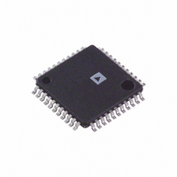
AD9042ASTZ Analog Devices Inc, AD9042ASTZ Datasheet - Page 13

AD9042ASTZ
Manufacturer Part Number
AD9042ASTZ
Description
IC ADC 12BIT 41MSPS 44-TQFP
Manufacturer
Analog Devices Inc
Datasheet
1.AD9042ASTZ.pdf
(24 pages)
Specifications of AD9042ASTZ
Data Interface
Parallel
Number Of Bits
12
Sampling Rate (per Second)
41M
Number Of Converters
3
Power Dissipation (max)
735mW
Voltage Supply Source
Analog and Digital, Dual ±
Operating Temperature
-40°C ~ 85°C
Mounting Type
Surface Mount
Package / Case
44-TQFP, 44-VQFP
Resolution (bits)
12bit
Sampling Rate
41MSPS
Input Channel Type
Single Ended
Supply Voltage Range - Analog
5V
Supply Voltage Range - Digital
5V
Supply Current
119mA
Number Of Elements
1
Resolution
12Bit
Architecture
Pipelined
Sample Rate
41MSPS
Input Polarity
Unipolar
Input Type
Voltage
Rated Input Volt
1.9/2.9V
Differential Input
No
Power Supply Requirement
Single
Single Supply Voltage (typ)
5V
Single Supply Voltage (min)
4.75V
Single Supply Voltage (max)
5.25V
Dual Supply Voltage (typ)
Not RequiredV
Dual Supply Voltage (min)
Not RequiredV
Dual Supply Voltage (max)
Not RequiredV
Power Dissipation
735mW
Differential Linearity Error
±1LSB
Integral Nonlinearity Error
±0.75LSB(Typ)
Operating Temp Range
-40C to 85C
Operating Temperature Classification
Industrial
Mounting
Surface Mount
Pin Count
44
Package Type
LQFP
Input Signal Type
Single-Ended
Lead Free Status / RoHS Status
Lead free / RoHS Compliant
Lead Free Status / RoHS Status
Lead free / RoHS Compliant, Lead free / RoHS Compliant
Available stocks
Company
Part Number
Manufacturer
Quantity
Price
Company:
Part Number:
AD9042ASTZ
Manufacturer:
Analog Devices Inc
Quantity:
10 000
Part Number:
AD9042ASTZ
Manufacturer:
ADI/亚德诺
Quantity:
20 000
THEORY OF OPERATION
The AD9042 analog-to-digital converter (ADC) employs a two-
stage subrange architecture. This design approach ensures
12-bit accuracy, without the need for laser trim, at low power.
As shown in Figure 1, the 1 V p-p single-ended analog input,
centered at 2.4 V, drives a single-input to differential-output
amplifier, A1. The output of A1 drives the first track-and-hold,
TH1. The high state of the ENCODE pulse places TH1 in hold
mode. The held value of TH1 is applied to the input of the 6-bit
coarse ADC. The digital output of the coarse ADC drives a 6-bit
DAC; the DAC is 12 bits accurate. The output of the 6-bit DAC
is subtracted from the delayed analog signal at the input to TH3
to generate a residue signal. TH2 is used as an analog pipeline
to null out the digital delay of the coarse ADC.
The residue signal is passed to TH3 on a subsequent clock cycle
where the signal is amplified by the residue amplifier, A2, and
converted to a digital word by the 7-bit residue ADC. One bit of
overlap is used to accommodate any linearity errors in the
coarse ADC.
The 6-bit coarse ADC word and 7-bit residue word are added
together and corrected in the digital error correction logic to
generate the output word. The result is a 12-bit parallel digital
word, which is CMOS-compatible, coded as twos complement.
ENCODING THE AD9042
The AD9042 is designed to interface with TTL and CMOS logic
families. The source used to drive the ENCODE pin(s) must be
clean and free from jitter. Sources with excessive jitter limit SNR
(see Equation 1 in the Noise Floor and SNR section).
The AD9042 encode inputs are connected to a differential input
stage (see Figure 21 in the Equivalent Circuits section). With no
input connected to either the ENCODE or input, the voltage
dividers bias the inputs to 1.6 V. For TTL or CMOS usage, the
encode source should be connected to ENCODE. ENCODE
should be decoupled using a low inductance or microwave chip
capacitor to ground. Devices such as the AVX 05085C103MA15, a
0.01 μF capacitor, work well.
If a logic threshold other than the nominal 1.6 V is required, the
following equations show how to use an external resistor, Rx, to
raise or lower the trip point (see Figure 21; R1 = 17 kΩ, R2 = 8 kΩ).
To lower the logic threshold, use the following equation:
V
1
=
R
1
TTL OR CMOS
R
Figure 25. Single-Ended TTL/CMOS Encode
2
+
SOURCE
5
R
R
1
2
R
R
X
0.01µF
X
+
R
2
R
X
ENCODE
ENCODE
AD9042
Rev. B | Page 13 of 24
To raise the logic threshold, use the following equation:
Although the single-ended encode works well for many
applications, driving the encode differentially provides increased
performance. Depending on circuit layout and system noise, a
1 dB to 3 dB improvement in SNR can be realized. It is not
recommended that differential TTL logic be used, however,
because most TTL families that support complementary
outputs are not delay or slew rate matched. Instead, it is
recommended that the encode signal be ac-coupled into the
ENCODE and ENCODE pins.
The simplest option is shown in Figure 28. The low jitter TTL
signal is coupled with a limiting resistor, typically 100 Ω, to the
primary side of an RF transformer (these transformers are
inexpensive and readily available; part number in Figure 28 is
from Mini-Circuits). The secondary side is connected to the
ENCODE and ENCODE pins of the converter. Because both
encode inputs are self-biased, no additional components are
required.
V
1
=
R
TTL
0.01µF
2
ENCODE
SOURCE
ENCODE
SOURCE
Figure 26. Lower Logic Threshold for Encode
+
Figure 27. Raise Logic Threshold for Encode
Figure 28. TTL Source Differential Encode
5
R
R
100Ω
R
1
2
0.01µF
1
+
R
R
X
R
R
V
X
AV
X
L
T1-1T
X
V
CC
L
ENCODE
ENCODE
ENCODE
ENCODE
AD9042
AD9042
ENCODE
ENCODE
AD9042
5V
5V
R1
R2
R1
R2
AD9042


