CS5342-CZZ Cirrus Logic Inc, CS5342-CZZ Datasheet - Page 17

CS5342-CZZ
Manufacturer Part Number
CS5342-CZZ
Description
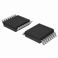
IC ADC AUD 105DB 200KHZ 16-TSSOP
Manufacturer
Cirrus Logic Inc
Datasheet
1.CS5342-CZZ.pdf
(21 pages)
Specifications of CS5342-CZZ
Data Interface
Serial
Number Of Bits
24
Sampling Rate (per Second)
200k
Number Of Converters
2
Voltage Supply Source
Analog and Digital
Operating Temperature
-10°C ~ 70°C
Mounting Type
Surface Mount
Package / Case
16-TSSOP
Resolution (bits)
24bit
Sampling Rate
192kSPS
Input Channel Type
Single Ended
Supply Voltage Range - Analog
3.1V To 5.25V
Supply Current
21mA
Digital Ic Case Style
TSSOP
Lead Free Status / RoHS Status
Lead free / RoHS Compliant
Other names
598-1688
Available stocks
Company
Part Number
Manufacturer
Quantity
Price
Part Number:
CS5342-CZZ
Manufacturer:
CIRRUS
Quantity:
20 000
DS608F1
4.4
4.5
4.6
4.7
4.8
Power-Up Sequence
Reliable power-up can be accomplished by keeping the device in reset until the power supplies, clocks and
configuration pins are stable. It is also recommended that reset be enabled if the analog or digital supplies
drop below the minimum specified operating voltages to prevent power-glitch-related issues.
Analog Connections
The analog modulator samples the input at 6.144 MHz. The digital filter rejects signals within the stopband
of the filter. However, there is no rejection for input signals that are multiples of the input sampling frequency
(n
at 6.144 MHz and provides the optimum source impedance for the modulators. The use of capacitors that
have a large voltage coefficient (such as general-purpose ceramics) must be avoided because these can
degrade signal linearity.
Grounding and Power Supply Decoupling
As with any high-resolution converter, the CS5342 requires careful attention to power supply and grounding
arrangements if its potential performance is to be realized.
rangements, with VA and VL connected to clean supplies. VD, which powers the digital filter, may be run
from the system logic supply or powered from the analog supply via a resistor. In this case, no additional
devices should be powered from VD. Decoupling capacitors should be as near to the ADC as possible, with
the low value ceramic capacitor being the nearest. All signals, especially clocks, should be kept away from
the FILT+ and VQ pins in order to avoid unwanted coupling into the modulators. The FILT+ and VQ decou-
pling capacitors, particularly the 0.1 µF, must be positioned to minimize the electrical path from FILT+ and
REF_GND. The CDB5342 evaluation board demonstrates the optimum layout and power supply arrange-
ments. To minimize digital noise, connect the ADC digital outputs only to CMOS inputs.
Synchronization of Multiple Devices
In systems where multiple ADCs are required, care must be taken to achieve simultaneous sampling. To
ensure synchronous sampling, the MCLK and LRCK must be the same for all of the CS5342’s in the system.
Capacitor Size on the Reference Pin (FILT+)
The CS5342 requires an external capacitance on the internal reference voltage pin, FILT+. The size of this
decoupling capacitor affects the low frequency distortion performance, as shown in
capacitor values used to optimize low frequency distortion performance. The THD+N curves in
×
6.144 MHz), where n=0, 1, 2, ....
AINx
Figure 21. CS5342 Recommended Analog Input Buffer
4.7 µF
100 kΩ
100 kΩ
VA
Figure 21
634 Ω
shows the suggested filter that attenuates any noise energy
C0G
470 pF
2700 pF
91 Ω
Figure 17
CS5342 AINx
shows the recommended power ar-
Figure
22, with larger
CS5342
Figure 22
17


