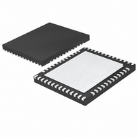
LTC2172CUKG-14#PBF Linear Technology, LTC2172CUKG-14#PBF Datasheet - Page 24

LTC2172CUKG-14#PBF
Manufacturer Part Number
LTC2172CUKG-14#PBF
Description
IC ADC 14BIT SER/PAR 65M 52-QFN
Manufacturer
Linear Technology
Datasheet
1.LTC2172IUKG-14PBF.pdf
(34 pages)
Specifications of LTC2172CUKG-14#PBF
Number Of Bits
14
Sampling Rate (per Second)
65M
Data Interface
Serial, Parallel
Number Of Converters
4
Power Dissipation (max)
419mW
Voltage Supply Source
Analog and Digital
Operating Temperature
0°C ~ 70°C
Mounting Type
Surface Mount
Package / Case
52-WFQFN Exposed Pad
Lead Free Status / RoHS Status
Lead free / RoHS Compliant
LTC2172-14/
LTC2171-14/LTC2170-14
APPLICATIONS INFORMATION
By default the outputs are standard LVDS levels: a 3.5mA
output current and a 1.25V output common mode volt-
age. An external 100Ω differential termination resistor
is required for each LVDS output pair. The termination
resistors should be located as close as possible to the
LVDS receiver.
The outputs are powered by OV
isolated from the A/D core power and ground.
Programmable LVDS Output Current
The default output driver current is 3.5mA. This current can
be adjusted by control register A2 in serial programming
mode. Available current levels are 1.75mA, 2.1mA, 2.5mA,
3mA, 3.5mA, 4mA and 4.5mA. In parallel programming
mode the SCK pin can select either 3.5mA or 1.75mA.
Optional LVDS Driver Internal Termination
In most cases, using just an external 100Ω termination
resistor will give excellent LVDS signal integrity. In addi-
tion, an optional internal 100Ω termination resistor can
be enabled by serially programming mode control register
A2. The internal termination helps absorb any refl ections
caused by imperfect termination at the receiver. When the
internal termination is enabled, the output driver current
is doubled to maintain the same output voltage swing. In
parallel programming mode the SDO pin enables internal
termination. Internal termination should only be used with
1.75mA, 2.1mA or 2.5mA LVDS output current modes.
Table 1. Maximum Sampling Frequency for All Serialization Modes. Note That These Limits Are for the LTC2172-14. The Sampling
Frequency for the Slower Speed Grades Cannot Exceed 40MHz (LTC2171-14) or 25MHz (LTC2170-14).
SERIALIZATION MODE
2-Lane
2-Lane
2-Lane
1-Lane
1-Lane
1-Lane
24
16-Bit Serialization
14-Bit Serialization
12-Bit Serialization
16-Bit Serialization
14-Bit Serialization
12-Bit Serialization
DD
and OGND which are
MAXIMUM SAMPLING
FREQUENCY , f
62.5
65
65
65
65
65
S
(MHz)
DATA FORMAT
Table 2 shows the relationship between the analog input
voltage and the digital data output bits. By default the
output data format is offset binary. The 2’s complement
format can be selected by serially programming mode
control register A1.
Table 2. Output Codes vs Input Voltage
>1.000000V
+0.999878V
+0.999756V
+0.000122V
+0.000000V
–0.000122V
–0.000244V
–0.999878V
–1.000000V
≤–1.000000V
Digital Output Randomizer
Interference from the A/D digital outputs is sometimes
unavoidable. Digital interference may be from capacitive or
inductive coupling or coupling through the ground plane.
Even a tiny coupling factor can cause unwanted tones in
the ADC output spectrum. These unwanted tones can be
randomized by randomizing the digital output before it is
transmitted off chip, which reduces the unwanted tone
amplitude.
The digital output is randomized by applying an exclu-
sive-OR logic operation between the LSB and all other
data output bits. To decode, the reverse operation is
A
(2V RANGE)
DCO FREQUENCY
IN
+
– A
3.5 • f
4 • f
3 • f
8 • f
7 • f
6 • f
IN
–
S
S
S
S
S
S
11 1111 1111 1111
11 1111 1111 1111
11 1111 1111 1110
10 0000 0000 0001
10 0000 0000 0000
01 1111 1111 1111
01 1111 1111 1110
00 0000 0000 0001
00 0000 0000 0000
00 0000 0000 0000
(OFFSET BINARY)
FR FREQUENCY
D13-D0
0.5 • f
f
f
f
f
f
S
S
S
S
S
S
(2’s COMPLEMENT)
01 1111 1111 1111
01 1111 1111 1111
01 1111 1111 1110
00 0000 0000 0001
00 0000 0000 0000
11 1111 1111 1111
11 1111 1111 1110
10 0000 0000 0001
10 0000 0000 0000
10 0000 0000 0000
SERIAL DATA RATE
D13-D0
16 • f
14 • f
12 • f
8 • f
7 • f
6 • f
S
S
S
S
S
S
21721014fa


