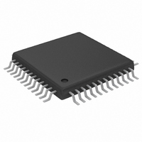
MAX1182ECM+D Maxim Integrated Products, MAX1182ECM+D Datasheet - Page 10

MAX1182ECM+D
Manufacturer Part Number
MAX1182ECM+D
Description
IC ADC 10BIT 65MSPS DUAL 48-TQFP
Manufacturer
Maxim Integrated Products
Datasheet
1.MAX1182ECMD.pdf
(21 pages)
Specifications of MAX1182ECM+D
Number Of Bits
10
Sampling Rate (per Second)
65M
Data Interface
Parallel
Number Of Converters
2
Power Dissipation (max)
240mW
Voltage Supply Source
Single Supply
Operating Temperature
-40°C ~ 85°C
Mounting Type
Surface Mount
Package / Case
48-TQFP Exposed Pad, 48-eTQFP, 48-HTQFP, 48-VQFP
Conversion Rate
65 MSPs
Resolution
10 bit
Snr
59.5 dB
Voltage Reference
2.048 V
Supply Voltage (max)
3.6 V
Supply Voltage (min)
2.7 V
Maximum Power Dissipation
2430 mW
Maximum Operating Temperature
+ 85 C
Mounting Style
SMD/SMT
Input Voltage
3 V
Minimum Operating Temperature
- 40 C
Lead Free Status / RoHS Status
Lead free / RoHS Compliant
Dual 10-Bit, 65Msps, 3V, Low-Power ADC
with Internal Reference and Parallel Outputs
10
______________________________________________________________________________________
31, 34
32, 33
PIN
21
22
23
24
25
26
27
28
29
30
35
36
37
38
39
40
41
42
43
44
45
46
47
48
—
REFOUT
NAME
OGND
REFIN
OV
REFN
REFP
D9B
D8B
D7B
D6B
D5B
D4B
D3B
D2B
D1B
D0B
D0A
D1A
D2A
D3A
D4A
D5A
D6A
D7A
D8A
D9A
EP
DD
Three-State Digital Output, Bit 9 (MSB), Channel B
Three-State Digital Output, Bit 8, Channel B
Three-State Digital Output, Bit 7, Channel B
Three-State Digital Output, Bit 6, Channel B
Three-State Digital Output, Bit 5, Channel B
Three-State Digital Output, Bit 4, Channel B
Three-State Digital Output, Bit 3, Channel B
Three-State Digital Output, Bit 2, Channel B
Three-State Digital Output, Bit 1, Channel B
Three-State Digital Output, Bit 0 (LSB), Channel B
Output Driver Ground
Output Driver Supply Voltage. Bypass each supply pin to OGND with a 0.1µF capacitor.
Output driver supply accepts a 1.7V to 3.6V input range.
Three-State Digital Output, Bit 0 (LSB), Channel A
Three-State Digital Output, Bit 1, Channel A
Three-State Digital Output, Bit 2, Channel A
Three-State Digital Output, Bit 3, Channel A
Three-State Digital Output, Bit 4, Channel A
Three-State Digital Output, Bit 5, Channel A
Three-State Digital Output, Bit 6, Channel A
Three-State Digital Output, Bit 7, Channel A
Three-State Digital Output, Bit 8, Channel A
Three-State Digital Output, Bit 9 (MSB), Channel A
Internal Reference Voltage Output. May be connected to REFIN through a resistor or a resistor
divider.
Reference Input. V
Positive Reference Input/Output. Conversion range is ± (V
> 0.1µF capacitor.
Negative Reference Input/Output. Conversion range is ± (V
a > 0.1µF capacitor.
Exposed Paddle. Connect to analog ground.
REFIN
= 2 x (V
REFP
- V
REFN
FUNCTION
). Bypass to GND with a > 1nF capacitor.
Pin Description (continued)
REFP
REFP
- V
- V
REFN
REFN
). Bypass to GND with a
). Bypass to GND with


