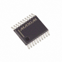
MAX1066BCUP+ Maxim Integrated Products, MAX1066BCUP+ Datasheet - Page 11

MAX1066BCUP+
Manufacturer Part Number
MAX1066BCUP+
Description
IC ADC 14-BIT 165KSPS 20-TSSOP
Manufacturer
Maxim Integrated Products
Datasheet
1.MAX1066BCUP.pdf
(14 pages)
Specifications of MAX1066BCUP+
Number Of Bits
14
Sampling Rate (per Second)
165k
Data Interface
Parallel
Number Of Converters
1
Power Dissipation (max)
16mW
Voltage Supply Source
Single Supply
Operating Temperature
0°C ~ 70°C
Mounting Type
Surface Mount
Package / Case
20-TSSOP
Number Of Adc Inputs
1
Architecture
SAR
Conversion Rate
165 KSPs
Resolution
14 bit
Input Type
Single-Ended Input
Interface Type
Parallel
Voltage Reference
Internal 4.096 V or External
Supply Voltage (max)
5.25 V
Supply Voltage (min)
2.7 V
Maximum Power Dissipation
879 mW
Maximum Operating Temperature
+ 70 C
Mounting Style
SMD/SMT
Minimum Operating Temperature
0 C
Lead Free Status / RoHS Status
Lead free / RoHS Compliant
Figure 7. MAX1065/MAX1066 Reference Adjust Circuit
EOC is provided to flag the microprocessor when a con-
version is complete. The falling edge of EOC signals
that the data is valid and ready to be output to the bus.
D0–D13 are the parallel outputs of the MAX1065/
MAX1066. These three-state outputs allow for direct
connection to a microcontroller I/O bus. The outputs
remain high-impedance during acquisition and conver-
sion. Data is loaded onto the bus with the third falling
edge of CS with R/C high after t
forces the output bus back to high-impedance. The
MAX1065/MAX1066 then waits for the next falling edge
of CS to start the next conversion cycle (Figure 2).
The MAX1065 loads the conversion result onto a 14-bit-
wide data bus while the MAX1066 has a byte-wide out-
put format. HBEN toggles the output between the
most/least significant byte. The least significant byte is
loaded onto the output bus when HBEN is low and the
most significant byte is on the bus when HBEN is high
(Figure 2).
Toggle RESET with CS high. The next falling edge of
CS will begin acquisition. This reset is an alternative to
the dummy conversion explained in the Starting a
Conversion section.
Figure 8 shows the MAX1065/MAX1066 output transfer
function. The output is coded in standard binary.
Most applications require an input buffer amplifier to
achieve 14-bit accuracy. If the input signal is multiplexed,
the input channel should be switched immediately after
acquisition, rather than near the end of or after a conver-
sion. This allows more time for the input buffer amplifier to
respond to a large step-change in input signal. The input
amplifier must have a high enough slew rate to complete
Low-Power, 14-Bit Analog-to-Digital Converters
100kΩ
5V
150kΩ
Reading the Conversion Result
______________________________________________________________________________________
68kΩ
0.22μF
DO
Transfer Function
ns. Bringing CS high
REFADJ
MAX1065
MAX1066
Input Buffer
RESET
the required output voltage change before the beginning
of the acquisition time. At the beginning of acquisition, the
internal sampling capacitor array connects to AIN (the
amplifier output) causing some output disturbance.
Ensure that the sampled voltage has settled to within the
required limits before the end of the acquisition time. If
the frequency of interest is low, AIN can be bypassed
with a large enough capacitor to charge the internal sam-
pling capacitor with very little ripple. However, for AC use,
AIN must be driven by a wideband buffer (at least
10MHz), which must be stable with the ADC’s capacitive
load (in parallel with any AIN bypass capacitor used) and
also settle quickly. An example of this circuit using the
MAX4434 is given in Figure 9.
Figure 8. MAX1065/MAX1066 Transfer Function
Figure 9. MAX1065/MAX1066 Fast Settling Input Buffer
with Parallel Interface
ANALOG
INPUT
11...111
11...110
11...101
00...011
00...010
00...001
00...000
OUTPUT CODE
0
1
MAX4434
2
INPUT VOLTAGE (LSB)
3
FULL-SCALE
TRANSITION
10Ω
FS - 3/2LSB
AIN
1LSB =
MAX1065/
FS = V
MAX1066
FS
16384
REF
V
REF
40pF
11


