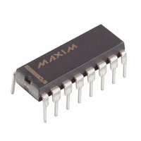
MAX1249BCPE+ Maxim Integrated Products, MAX1249BCPE+ Datasheet - Page 18

MAX1249BCPE+
Manufacturer Part Number
MAX1249BCPE+
Description
IC ADC 4CH 10BIT 133KSPS 16-DIP
Manufacturer
Maxim Integrated Products
Datasheet
1.MAX1249BCPE.pdf
(24 pages)
Specifications of MAX1249BCPE+
Number Of Bits
10
Sampling Rate (per Second)
133k
Data Interface
MICROWIRE™, QSPI™, Serial, SPI™
Number Of Converters
1
Power Dissipation (max)
3.6mW
Voltage Supply Source
Single Supply
Operating Temperature
0°C ~ 70°C
Mounting Type
Through Hole
Package / Case
16-DIP (0.300", 7.62mm)
Lead Free Status / RoHS Status
Lead free / RoHS Compliant
+2.7V to +5.25V, Low-Power, 4-Channel,
Serial 10-Bit ADCs in QSOP-16
With both the MAX1248 and MAX1249, an external ref-
erence can be placed at either the input (REFADJ) or
the output (VREF) of the internal reference-buffer ampli-
fier. The REFADJ input impedance is typically 20kΩ for
the MAX1248 and higher than 100kΩ for the MAX1249,
where the internal reference is omitted. At VREF, the
DC input resistance is a minimum of 18kΩ. During con-
version, an external reference at VREF must deliver
up to 350µA DC load current and have an output
impedance of 10Ω or less. If the reference has higher
output impedance or is noisy, bypass it close to the
VREF pin with a 4.7µF capacitor.
Using the REFADJ input makes buffering the external
reference unnecessary. To use the direct VREF input,
disable the internal buffer by tying REFADJ to V
power-down, the input bias current to REFADJ can be
as much as 25µA with REFADJ tied to V
REFADJ to AGND to minimize the input bias current in
power-down.
Table 7 shows the full-scale voltage ranges for unipolar
and bipolar modes.
The external reference must have a temperature coeffi-
cient of 20ppm/°C or less to achieve accuracy to within
1LSB over the commercial temperature range of 0°C to
+70°C.
Figure 16 depicts the nominal, unipolar input/output
(I/O) transfer function, and Figure 17 shows the bipolar
input/output transfer function. Code transitions occur
halfway between successive-integer LSB values.
Output coding is binary, with 1LSB = 2.44mV (2.500V /
1024) for unipolar operation and 1LSB = 2.44mV
[(2.500V / 2 - -2.500V / 2) / 1024] for bipolar operation.
18
Figure 14. MAX1248 FULLPD/FASTPD Power-Up Sequence
______________________________________________________________________________________
DIN
VREF
REFADJ
1
FULLPD
1.21V
2.50V
0V
0V
0 0
(ZEROS)
Transfer Function
External Reference
COMPLETE CONVERSION SEQUENCE
1
= RC = 20k x C
FASTPD
DD
DD
1.6ms WAIT
. Pull
0 1
. In
REFADJ
Figure 15. MAX1248 Reference-Adjust Circuit
Figure 16. Unipolar Transfer Function, Full Scale (FS) = VREF
+ COM, Zero Scale (ZS) = COM
t
BUFFEN
11 . . . 111
11 . . . 110
00 . . . 011
00 . . . 010
11 . . . 101
00 . . . 001
00 . . . 000
1
NOPD
CH1
OUTPUT CODE
75µs
(COM)
100k
24k
1
0
1
+3.3V
1
INPUT VOLTAGE (LSBs)
2
1
FULLPD
3
CH7
510k
0 0
0.01µF
FULL-SCALE
TRANSITION
(ZEROS)
FS - 3/2LSB
9
1
REFADJ
MAX1248
FASTPD
FS = VREF + COM
ZS = COM
1LSB =
0 1
FS
VREF
1024


