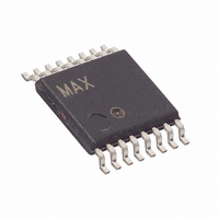
MAX1153BEUE+ Maxim Integrated Products, MAX1153BEUE+ Datasheet - Page 20

MAX1153BEUE+
Manufacturer Part Number
MAX1153BEUE+
Description
IC ADC 10BIT SYS MON 16TSSOP
Manufacturer
Maxim Integrated Products
Datasheet
1.MAX1153BEUE.pdf
(30 pages)
Specifications of MAX1153BEUE+
Number Of Bits
10
Sampling Rate (per Second)
94k
Data Interface
MICROWIRE™, QSPI™, Serial, SPI™
Number Of Converters
1
Power Dissipation (max)
6.6mW
Voltage Supply Source
Single Supply
Operating Temperature
-40°C ~ 85°C
Mounting Type
Surface Mount
Package / Case
16-TSSOP
Number Of Adc Inputs
10
Architecture
SAR
Conversion Rate
94 KSPs
Resolution
10 bit
Interface Type
Serial
Voltage Reference
Internal 2.5 V or External
Supply Voltage (max)
3.3 V
Mounting Style
SMD/SMT
Lead Free Status / RoHS Status
Lead free / RoHS Compliant
Stand-Alone, 10-Channel, 10-Bit System Monitors
with Internal Temperature Sensor and V
The scan mode bit selects between automatic scan-
ning and manual conversion mode.
When set (B2 = 1), the MAX1153/MAX1154 enter auto-
matic scanning mode and convert every enabled chan-
nel starting with the internal temperature sensor,
followed by the V
AIN0 to AIN7.
After converting all the enabled channels, the
MAX1153/MAX1154 enter a wait state set by the sam-
ple wait bits in the setup register. After completing the
sample wait time, the scan cycle repeats.
When B2 = 0, the MAX1153/MAX1154 are in manual
mode and convert only the selected channel after
receiving a Manually Triggered Conversion command
(see the Manually Triggered Conversion (Command
Code 0000) section). Whether in automatic scanning
mode or manual mode, a Read Current Data Register
for Selected Channel command outputs the last-com-
pleted conversion result for the addressed channel at
DOUT.
Table 10. Reference Selection
Table 11. Alarm Register Format
20
B1
B23/B22
0
0
1
1
TEMP
______________________________________________________________________________________
B0
0
1
0
1
Voltage measurements use external reference,
while temperature measurements use the internal
reference. A 20µs reference startup delay is
added prior to each temperature measurement
in this mode. This is the default mode after
power-up and after a software RESET.
All measurements use the internal reference. A
40µs reference startup delay is added prior to
starting the scanning of enabled channels,
allowing the internal reference to stabilize.
Note: For sample wait times less than 80µs, the
reference is continuously powered when in
automatic scan mode.
All measurements use the internal reference. By
selecting this mode, the reference is powered up
immediately when CS goes high after writing this
configuration. Once the reference system is
powered up, no further delay is added.
Reserved.
B21/B20
V
DD
DD
Setup Register: Scan Mode Bit (B2)
B19/B18
monitor, then sequencing through
AIN0
REFERENCE MODE
B17/B16
AIN1
B15/B14
AIN2
B13/B12
AIN3
B11/B10
The MAX1153/MAX1154 can be used with an internal
or external reference. Select between internal and
external reference modes through bits B1 and B0 of the
setup register (see Table 10).
The alarm register (Table 11) holds the current alarm sta-
tus for all of the monitored signals. This 24-bit register
can only be read and cleared. The alarm register has 2
bits for each external input channel, 2 for the onboard
temperature sensor, and 2 for the V
Table 12). At power-up, these bits are logic low, indicat-
ing no alarms at any input. When any bit in the alarm reg-
ister is set, INT becomes active and remains active until
all alarm bits are cleared. After a fault counter exceeds
the set threshold, the alarm register bits for that particular
channel are updated to indicate an alarm.
To clear the interrupt, reset the active alarm bit with the
Clear Alarm Register command, Clear Channel Alarm
command, a RESET command, or by writing a new
configuration to the faulting channel. The alarm register
defaults to 000000 hex.
Table 11 illustrates how the alarm register stores the
information on which channel a fault has occurred. The
alarm code for each bit pair is shown in Table 12.
Each channel (internal temperature sensor, V
tor, and AIN0 to AIN7) has registers to hold the conver-
sion result (current data register) and channel-specific
configuration data. The channel-specific configuration
registers include: the upper threshold register, the
lower threshold register, and the channel configuration
register. In differential mode, only the registers for the
even channel of the differential input pair are used. The
channel-specific configuration registers for the odd
channel of a differential channel pair are ignored.
Table 12. Alarm Register Coding
(2 Bits/Channel)
AIN4
CODE
Setup Register: Reference Selection Bits (B1, B0)
00
01
10
00
B9/B8
AIN5
No alarm (power-up state)
Input is below lower threshold
Input is above upper threshold
Reserved
B7/B6
AIN6
Channel Registers
DESCRIPTION
B5/B4
AIN7
DD
Alarm Register
Monitor
DD
B3/B2
Res
monitor (see
DD
B1/B0
Res
moni-


