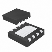
MAX1089ETA+T Maxim Integrated Products, MAX1089ETA+T Datasheet - Page 3

MAX1089ETA+T
Manufacturer Part Number
MAX1089ETA+T
Description
IC ADC 10BIT 150KSPS 8-TDFN
Manufacturer
Maxim Integrated Products
Datasheet
1.MAX1086ETAT.pdf
(15 pages)
Specifications of MAX1089ETA+T
Number Of Bits
10
Sampling Rate (per Second)
150k
Data Interface
MICROWIRE™, QSPI™, Serial, SPI™
Number Of Converters
1
Power Dissipation (max)
740µW
Voltage Supply Source
Single Supply
Operating Temperature
-40°C ~ 80°C
Mounting Type
Surface Mount
Package / Case
8-WDFN Exposed Pad
Number Of Adc Inputs
1
Architecture
SAR
Conversion Rate
150 KSPs
Resolution
10 bit
Input Type
Differential
Interface Type
3-Wire (SPI, QSPI, MICROWIRE)
Voltage Reference
External
Supply Voltage (max)
3.3 V
Maximum Power Dissipation
1454.5 mW
Maximum Operating Temperature
+ 85 C
Mounting Style
SMD/SMT
Minimum Operating Temperature
- 40 C
Lead Free Status / RoHS Status
Lead free / RoHS Compliant
Other names
MAX1089ETA+T
ELECTRICAL CHARACTERISTICS (continued)
(V
0.1µF capacitor at REF, f
noted. Typical values at T
ANALOG INPUT
Input Voltage Range (Note 4)
Input Leakage Current
Input Capacitance
Input Voltage Range
Input Current
DIGITAL INPUTS/OUTPUTS (SCLK, CNVST, DOUT)
Input Low Voltage
Input High Voltage
Input Leakage Current
Input Capacitance
Output Low Voltage
Output High Voltage
Three-State Leakage Current
Three-State Output Capacitance
POWER REQUIREMENTS
Positive Supply Voltage
Positive Supply Current
Positive Supply Rejection
EXTERNAL REFERENCE INPUT
1-Channel True-Differential ADCs in SOT23 and TDFN
DD
= +2.7V to +3.6V, V
PARAMETER
150ksps, 10-Bit, 2-Channel Single-Ended, and
_______________________________________________________________________________________
SCLK
A
REF
= +25°C.)
= +2.5V for MAX1087/MAX1089, or V
= 8MHz (50% duty cycle), AIN- = GND for MAX1088/MAX1089. T
SYMBOL
C
V
I
V
V
PSR
V
C
V
I
REF
V
OUT
REF
DD
I
OH
OL
DD
IH
IL
L
IN
Unipolar
Bipolar
C hannel not sel ected or conver si on stop p ed
V
V
Acquisition/Between conversions
I
I
I
CNVST = GND
CNVST = GND
MAX1086/MAX1088
MAX1087/MAX1089
V
V
Shutdown
V
V
SINK
SINK
SOURCE
REF
REF
DD
DD
DD
DD
= +3V
= +5V
= 5V ±5%; full-scale input
= +2.7V to +3.6V; full-scale input
= +2.5V at 150ksps
= +4.096V at 150ksps
= 2mA
= 4mA
= 1.5mA
CONDITIONS
DD
= +4.75V to +5.25V, V
f
f
f
f
f
f
f
f
SAMPLE
SAMPLE
SAMPLE
SAMPLE
SAMPLE
SAMPLE
SAMPLE
SAMPLE
=150ksps
=100ksps
=10ksps
=1ksps
=150ksps
=100ksps
=10ksps
=1ksps
REF
-V
V
A
= +4.096V for MAX1086/MAX1088,
MIN
V
4.75
REF
DD
-0.5
1.0
2.7
= T
DD
0
-1
/2
MIN
±0.01
±0.01
to T
TYP
±0.1
±0.1
245
150
320
215
5.0
3.0
2.5
0.2
34
16
26
15
15
15
22
2
MAX,
+50mV
V
MAX
V
unless otherwise
V
±0.1
5.25
±1.2
REF
±10
350
400
0.8
0.4
0.8
3.6
1.0
±1
30
45
±1
REF
DD
5
/2
UNITS
mV
µA
pF
µA
µA
pF
µA
pF
µA
V
V
V
V
V
V
V
V
3


