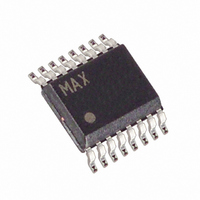
MAX1111EEE+ Maxim Integrated Products, MAX1111EEE+ Datasheet - Page 12

MAX1111EEE+
Manufacturer Part Number
MAX1111EEE+
Description
IC ADC 8BIT LP 16-QSOP
Manufacturer
Maxim Integrated Products
Datasheet
1.MAX1111CEE.pdf
(20 pages)
Specifications of MAX1111EEE+
Number Of Bits
8
Sampling Rate (per Second)
50k
Data Interface
MICROWIRE™, QSPI™, Serial, SPI™
Number Of Converters
1
Power Dissipation (max)
667mW
Voltage Supply Source
Single Supply
Operating Temperature
0°C ~ 70°C
Mounting Type
Surface Mount
Package / Case
16-SSOP (0.150", 3.90mm Width)
Number Of Adc Inputs
8
Architecture
SAR
Conversion Rate
50 KSPs
Resolution
8 bit
Input Type
Differential
Interface Type
4-Wire (SPI, QSPI, MICROWIRE)
Voltage Reference
Internal 2.048 V or External
Supply Voltage (max)
5 V
Maximum Power Dissipation
667 mW
Maximum Operating Temperature
+ 85 C
Mounting Style
SMD/SMT
Input Voltage
1.5 V
Minimum Operating Temperature
- 40 C
Lead Free Status / RoHS Status
Lead free / RoHS Compliant
+2.7V, Low-Power, Multichannel,
Serial 8-Bit ADCs
Figure 6. Common Serial-Interface Connections to the
MAX1110/MAX1111
Figure 7. Single-Conversion Timing, External Clock Mode, 24 Clocks
12
SSTRB
DOUT
A/D STATE
SCLK
DIN
CS
______________________________________________________________________________________
a) SPI
b) QSPI
c) MICROWIRE
START
1
MISO
MISO
SCK
SCK
SEL2 SEL1 SEL0
I/O
CS
I/O
SS
SS
SK
SI
IDLE
RB1
+3V
+3V
4
UNI/
BIP
SGL/
DIF
(f
ACQUISITION
SCLK
PD1
CS
SCLK
DOUT
CS
SCLK
DOUT
CS
SCLK
DOUT
t
4µs
ACQ
= 500kHz)
PD0
MAX1110
MAX1111
MAX1110
MAX1111
MAX1110
MAX1111
8
B7
B6
12
RB2
Make sure the CPU’s serial interface runs in master
mode so the CPU generates the serial clock. Choose a
clock frequency from 50kHz to 500kHz.
1) Set up the control byte for external clock mode and
2) Use a general-purpose I/O line on the CPU to pull
3) Transmit TB1 and, simultaneously, receive a byte
4) Transmit a byte of all zeros ($00 hex) and, simulta-
5) Transmit a byte of all zeros ($00 hex) and, simulta-
6) Pull CS high.
Figure 7 shows the timing for this sequence. Bytes RB2
and RB3 contain the result of the conversion padded
with two leading zeros and six trailing zeros. The total
conversion time is a function of the serial-clock
frequency and the amount of idle time between 8-bit
transfers. Make sure that the total conversion time does
not exceed 1ms, to avoid excessive T/H droop.
CS, SCLK, and DIN can accept input signals up to
5.5V, regardless of the supply voltages. This allows the
MAX1110/MAX1111 to accept digital inputs from both
3V and 5V systems.
B5
CONVERSION
call it TB1. TB1 should be of the format 1XXXXX11
binary, where the Xs denote the particular channel
and conversion mode selected.
CS low.
and call it RB1. Ignore RB1.
neously, receive byte RB2.
neously, receive byte RB3.
B4
B3
B2
16
B1
B0
FILLED WITH ZEROS
Simple Software Interface
20
RB3
IDLE
Digital Inputs
24


