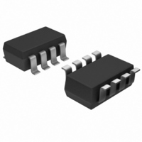
MAX1036EKA+T Maxim Integrated Products, MAX1036EKA+T Datasheet - Page 8

MAX1036EKA+T
Manufacturer Part Number
MAX1036EKA+T
Description
IC ADC 8-BIT 188KSPS SOT23-8
Manufacturer
Maxim Integrated Products
Datasheet
1.MAX1037EKAT.pdf
(23 pages)
Specifications of MAX1036EKA+T
Number Of Bits
8
Sampling Rate (per Second)
188k
Data Interface
I²C, Serial
Number Of Converters
1
Power Dissipation (max)
1.75mW
Voltage Supply Source
Single Supply
Operating Temperature
-40°C ~ 85°C
Mounting Type
Surface Mount
Package / Case
SOT-23-8
Number Of Adc Inputs
4
Conversion Rate
188 KSPs
Resolution
8 bit
Interface Type
Serial (2-Wire, I2C)
Snr
49 dB
Voltage Reference
4.096 V
Supply Voltage (max)
5.5 V
Supply Voltage (min)
4.5 V
Maximum Power Dissipation
567 mW
Maximum Operating Temperature
+ 85 C
Mounting Style
SMD/SMT
Input Voltage
5 V
Minimum Operating Temperature
- 40 C
Lead Free Status / RoHS Status
Lead free / RoHS Compliant
Other names
MAX1036EKA+TTR
The MAX1036–MAX1039 ADCs use successive-
approximation conversion techniques and input T/H cir-
cuitry to capture and convert an analog signal to a
serial 8-bit digital output. The MAX1036/MAX1037 are
4-channel ADCs, and the MAX1038/MAX1039 are 12-
channel ADCs. These devices feature a high-speed 2-
wire serial interface supporting data rates up to
1.7MHz. Figure 3 shows the simplified functional dia-
gram for the MAX1038/MAX1039.
The MAX1036–MAX1039 operate from a single supply
and consume 350µA at sampling rates up to 188ksps.
The MAX1037/MAX1039 feature a 2.048V internal
reference and the MAX1036/MAX1038 feature a 4.096V
internal reference. All devices can be configured for
use with an external reference from 1V to V
The MAX1036–MAX1039 analog input architecture con-
tains an analog input multiplexer (MUX), a T/H capaci-
tor, T/H switches, a comparator, and a switched
capacitor digital-to-analog converter (DAC) (Figure 4).
In single-ended mode, the analog input multiplexer con-
nects C
the Configuration/Setup Bytes (Write Cycle) section). The
charge on C
pseudo-differential mode, the analog input multiplexer
connects C
CS[3:0]. The charge on C
log input when converted.
2.7V to 3.6V and 4.5V to 5.5V, Low-Power,
4-/12-Channel 2-Wire Serial 8-Bit ADCs
8
_______________________________________________________________________________________
MAX1036/
MAX1037
1, 2, 3
T/H
—
—
—
4
5
6
7
8
to the analog input selected by CS[3:0] (see
T/H
T/H
PIN
is referenced to GND when converted. In
to the ‘+’ analog input selected by
Analog Input and Track/Hold
5, 4, 3, 2, 1
MAX1038/
MAX1039
16, 15, 14
Detailed Description
8, 7, 6
13
10
11
12
—
T/H
9
is referenced to the ‘-’ ana-
AIN8–AIN10
Power Supply
AIN0–AIN2
AIN3–AIN7
AIN11/REF
AIN3/REF
NAME
GND
SDA
SCL
V
DD
DD
.
Analog Inputs
Analog Input 3/Reference Input or Output. Selected in the setup
register.
Analog Input 11/Reference Input or Output. Selected in the setup
register.
Clock Input
Data Input/Output
Ground
Positive Supply. Bypass to GND with a 0.1µF capacitor.
The MAX1036–MAX1039 input configuration is pseudo-
differential in that only the signal at the ‘+’ analog input
is sampled with the T/H circuitry. The ‘-’ analog input
signal must remain stable within ±0.5LSB (±0.1LSB for
best results) with respect to GND during a conversion.
To accomplish this, connect a 0.1µF capacitor from ‘-’
analog input to GND. See the Single-Ended/Pseudo-
Differential Input section.
During the acquisition interval, the T/H switches are in
the track position and C
signal. At the end of the acquisition interval, the T/H
switches move to the hold position retaining the charge
on C
During the conversion interval, the switched capacitive
DAC adjusts to restore the comparator input voltage to
zero within the limits of 8-bit resolution. This action
requires eight conversion clock cycles and is equiva-
lent to transferring a charge of 18pF
from C
ing a digital representation of the analog input signal.
Sufficiently low source impedance is required to ensure
an accurate sample. A source impedance below 1.5kΩ
does not significantly degrade sampling accuracy. To
minimize sampling errors with higher source imped-
ances, connect a 100pF capacitor from the analog
input to GND. This input capacitor forms an RC filter
with the source impedance limiting the analog input
bandwidth. For larger source impedances, use a buffer
amplifier to maintain analog input signal integrity.
When operating in internal clock mode, the T/H circuitry
enters its tracking mode on the ninth falling clock edge
T/H
T/H
as a sample of the input signal.
to the binary weighted capacitive DAC form-
FUNCTION
T/H
charges to the analog input
Pin Description
(V
IN
+ - V
IN
-)


