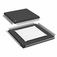
AD9446BSVZ-100 Analog Devices Inc, AD9446BSVZ-100 Datasheet - Page 28

AD9446BSVZ-100
Manufacturer Part Number
AD9446BSVZ-100
Description
IC ADC 16BIT 100MSPS 100-TQFP
Manufacturer
Analog Devices Inc
Datasheet
1.AD9446BSVZ-100.pdf
(36 pages)
Specifications of AD9446BSVZ-100
Data Interface
Parallel
Number Of Bits
16
Sampling Rate (per Second)
100M
Number Of Converters
1
Power Dissipation (max)
2.8W
Voltage Supply Source
Single Supply
Operating Temperature
-40°C ~ 85°C
Mounting Type
Surface Mount
Package / Case
100-TQFP Exposed Pad
Resolution (bits)
16bit
Sampling Rate
100MSPS
Input Channel Type
Differential, Single Ended
Supply Voltage Range - Digital
3V To 3.6V
Supply Current
368mA
Number Of Elements
1
Resolution
16Bit
Architecture
Pipelined
Sample Rate
100MSPS
Input Polarity
Bipolar
Input Type
Voltage
Rated Input Volt
±1/±1.6V
Differential Input
Yes
Power Supply Requirement
Single
Single Supply Voltage (typ)
3.3/5V
Single Supply Voltage (min)
3.14/4.75V
Single Supply Voltage (max)
3.46/5.25V
Dual Supply Voltage (typ)
Not RequiredV
Dual Supply Voltage (min)
Not RequiredV
Dual Supply Voltage (max)
Not RequiredV
Power Dissipation
2.8W
Differential Linearity Error
±0.85LSB
Integral Nonlinearity Error
±6LSB
Operating Temp Range
-40C to 85C
Operating Temperature Classification
Industrial
Mounting
Surface Mount
Pin Count
100
Package Type
TQFP EP
Input Signal Type
Differential
Package
100TQFP EP
Number Of Analog Inputs
1
Digital Interface Type
Parallel
Signal To Noise Ratio
79.7(Typ) dB
Lead Free Status / RoHS Status
Lead free / RoHS Compliant
For Use With
AD9446-80LVDS/PCBZ - BOARD EVALUATION AD9446-80
Lead Free Status / Rohs Status
Compliant
Available stocks
Company
Part Number
Manufacturer
Quantity
Price
Company:
Part Number:
AD9446BSVZ-100
Manufacturer:
AD
Quantity:
138
Company:
Part Number:
AD9446BSVZ-100
Manufacturer:
ADI
Quantity:
132
Part Number:
AD9446BSVZ-100
Manufacturer:
ADI/亚德诺
Quantity:
20 000
AD9446
OPERATIONAL MODE SELECTION
Data Format Select
The data format select (DFS) pin of the AD9446 determines
the coding format of the output data. This pin is 3.3 V CMOS
compatible, with logic high (or AVDD1, 3.3 V) selecting twos
complement and DFS logic low (AGND) selecting offset binary
format. Table 10 summarizes the output coding.
Output Mode Select
The OUPUT MODE pin controls the logic compatibility,
as well as the pinout of the digital outputs. This pin is a CMOS-
Table 10. Digital Output Coding
Code
65,536
32,768
32,767
0
VIN+ − VIN−
Input Span = 3.2 V p-p (V)
+1.600
0
−0.0000488
−1.60
VIN+ − VIN−
Input Span = 2 V p-p (V)
+1.000
0
−0.000122
−1.00
Rev. 0 | Page 28 of 36
Digital Output
Offset Binary (D15••••••D0)
1111 1111 1111 1111
1000 0000 0000 0000
0111 1111 1111 1111
0000 0000 0000 0000
compatible input. With OUTPUT MODE = 0 (AGND), the
AD9446 outputs are CMOS compatible, and the pin assignment
for the device is as defined in Table 8. With OUTPUT MODE = 1
(AVDD1, 3.3 V), the AD9446 outputs are LVDS compatible, and
the pin assignment for the device is as defined in Table 7.
Duty Cycle Stabilizer
The DCS circuit is controlled by the DCS MODE pin; a CMOS
logic low (AGND) on DCS MODE enables the DCS, and logic
high (AVDD1, 3.3 V) disables the controller.
Digital Output
Twos Complement (D15••••••D0)
0111 1111 1111 1111
0000 0000 0000 0000
1111 1111 1111 1111
1000 0000 0000 0000


